32 www.xilinx.com ML361 Virtex-II Pro Memory Board
UG060 (v1.2) November 8, 2007
Chapter 4: Signal Integrity Recommendations and Simulations
R
Data Signals from the FPGA to Memory (SSTL2_C2 at FPGA)
The simulations in this subsection test the data signals from the FPGA to memory.
Simulations were performed for the following cases: typical, slow weak, fast strong. An
eye diagram is provided also.
Typical Case Simulation for Data Signals from the FPGA to the Last DDR
Component
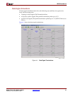
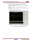
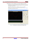
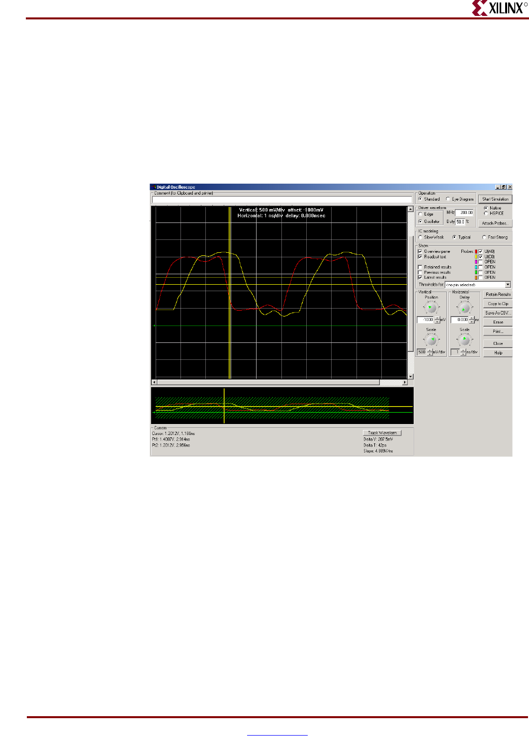
For the typical case simulation, the resulting duty cycle is 47.24/52.62. Figure 4-2 shows
the simulation screen capture for the typical case.
X-Ref Target - Figure 4-2
Figure 4-2: Data Signal from FPGA to Memory (Typical Case)
ug060_c5_02_091003


