ML361 Virtex-II Pro Memory Board www.xilinx.com 67
UG060 (v1.2) November 8, 2007
Providing Additional Ground Pins
R
Providing Additional Ground Pins
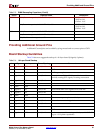
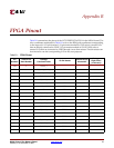
Additional Ground pins can be added by tying unused and no connect pins to GND.
Board Stackup Guidelines
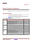
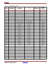
Table 5-4 shows a suggested stackup of a 16-layer board (8 signals, 8 planes).
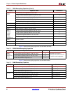
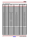
VREF 0.01 µF ceramic capacitor, 0402 6V X7R –20/+20% 1 VREF to GND
1 VREF to 2.6V
1 GND to 2.6V
0.1 µF ceramic capacitor, 0603 6V X7R –20/+20% 1 VREF to GND
1 VREF to 2.6V
1 GND to 2.6V
VSS 0.01 µF ceramic capacitor, 0402 6V X7R –20/+20% 8
0.1 µF ceramic capacitor, 0603 6V X7R –20/+20% 4
330 µF solid tantalum capacitor, 6.3V 1
Table 5-3: DIMM Decoupling Capacitors (Cont’d)
Pin(s) Capacitor Value Distribution
Table 5-4: 16-Layer Board Stackup
# Type Layer Trace / Spacing Comments
1 Signal TOP 8 mil, 8 mil
2Plane GND GND
3 Plane +2.5V +2.5V separate plane
4 Signal-X IN1 5 mil, 5 mil Route clocks on IN1 and IN2 layers. Can be used for
carefully routing SSTL signals, if routing area needed
5 Signal-Y IN2 5 mil, 5 mil
6Plane +2.6V
7Plane GND
8 Signal-X IN3 5 mil, 5 mil Route all 200 MHz SSTL signals on IN3 and IN4
9 Signal-Y IN4 5 mil, 5 mil
10 Plane GND
11 Plane +1.3V & +1.5V Carve out two power planes on this layer
12 Signal-X IN5 5 mil, 5 mil Route other non-critical signals here
13 Signal-Y IN6 5 mil, 5 mil
14 Plane +3.3V
15 Plane GND
16 Signal BOT 8 mil, 8 mil In the area not used for routing on this layer, add GND fill
to give +3.3V planar capacitance.


