


e-STUDIO350/352/353/450/452/453
DRUM RELATED SECTION
11
11 - 5
© 2003 - 2008 TOSHIBA TEC CORPORATION All rights reserved
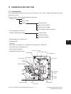
11.3 Output Control Circuits of High-Voltage Transformer
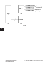
11.3.1 Overview
• Generate the output control voltage Vc of the main charger, transfer/separation charger, transfer
guide bias and developer bias.
• Convert Vc
The current is output linearly.
11.3.2 Description of operations
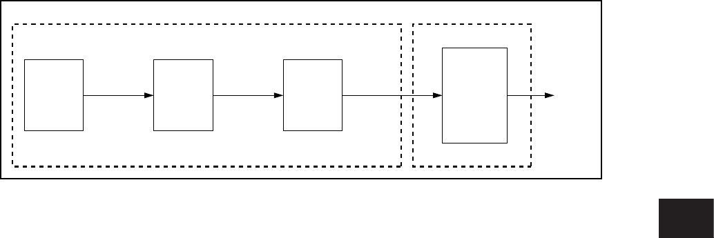
• Outputs the adjustment value of the main, transfer and separation chargers, developer bias and
transfer guide bias in the NVRAM to the ASIC GA.
↓
• Outputs the control voltage data from the ASIC GA to the D/A converter.
↓
• Converts to the analog data by the D/A converter.
↓
• Outputs the control voltage Vc to the main, transfer and separation chargers, developer bias and
transfer guide bias transformer.
↓
• The main, transfer and separation chargers, developer bias and transfer guide bias transformer gen
-
erate output current or voltage which is proportional to the control voltage Vc.
* Adjustment of the control voltage Vc (change of adjustment data) is performed in the adjustment
mode (05).
* Theoutputvalueofthetransferguidebiasisxedwhenthehigh-voltagetransformerisshipped
from the factory.
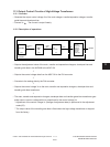
Fig. 11-301
HVT board
IC32
IC38
IC2
NVRAM
LGC board
ASIC
GA
Vc
Output
Main/
transfer/
separation/
chargers,
developer
bias and
transfer
guide bias
D/A
converter
Digital
data
Adjustment
value
Analog
04/01