


2
2 - 24e-STUDIO350/352/353/450/452/453
OUTLINE OF THE MACHINE
© 2003 - 2008 TOSHIBA TEC CORPORATION All rights reserved
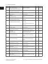
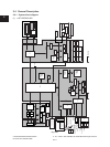
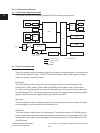
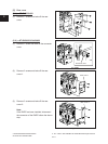
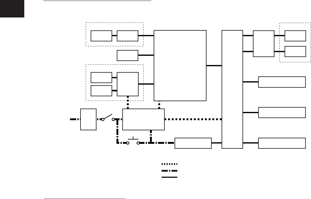
2.4.2 Construction of boards
(a) Construction diagram of boards
This system consists of the following including the SYS board as a main board.
SYS
PS-ACC
FIL
or
FUS
LGC
CCD
INV
SLG
Scanner unit
KEY
DSP
Control panel
NIC*
ADU
SFB
HVT
IH
LDR
LRL
SNS
Laser unit
:
DC power supply line
*
:
e-STUDIO350/450 only
:
AC power supply line
:
Signal line
AC input
Main switch
Cover opening/closing
interlock switch
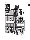
(b) Function of each board
CCD board:
Thisistheboardtoconvertthereectedlightbytheoriginaltoelectricalsignals.Itconsistsofthe
CCD,anditsperipheralcircuitry.TheCCDconvertsthereectedlightbytheoriginaltoanalog
signal and outputs it to the SLG board.
SLG board:
This is the board to mainly control the scanning function (scanner unit) and consists of the
Scanner-CPU, ASIC, memory (Flash ROM and SRAM), A/D converter, driver for motor drive,
etc. When scanning the original, the exposure lamp and scan motor are driven by the command
from the Scanner-CPU. The analog signal output from the CCD board is then converted to digital
signal by the A/D converter. Image processing is performed by ASIC.
INV board:
This is the board on which the lighting control circuit of the exposure lamp is mounted. The expo-
sure lamp lights by the command from the Scanner-CPU.
DSP board:
This is the board to mainly control the control panel. The panel processing CPU detecting the in-
put from each button and touch panel, and the lighting control circuit for the backlight of the LCD
are mounted. And it relays the control signal of the control panel from the SYS board to the LCD
and KEY board.
Fig. 2-402
05/11