


3 - 2
3
e-STUDIO350/352/353/450/452/453
COPY PROCESS
© 2003 - 2008 TOSHIBA TEC CORPORATION All rights reserved
3.2 Details of Copying Process
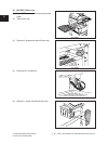
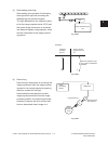
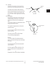
(1) Photoconductive drum
The photoconductive drum consists of two
layers. The outer layer is a photoconductive
layer made of an organic photoconductive
carrier (OPC), and the inner layer is an
aluminum conductive base in a cylindrical
form.
The photoconductor has the following
property: when it is exposed to light, the
electrical resistance it possesses increases
or decreases according to the strength of the
light.
Example:
· Strong lighten
Resistance is decreased (works as a
conductor.)
· Weak lighten
Resistance is increased (works as an
insulator.)
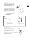
[Formation of electrostatic latent image]
In the processes of charging, data reading,
data writing, discharging described later,
negative potential of the areas on the drum
corresponding to black areas of the original
are eliminated, while the areas on the drum
corresponding to white areas retains the
negative charge.
As this image on the drum formed by the
negative potential is not visible, it is called an
“electrostatic latent image.”(2) Charging
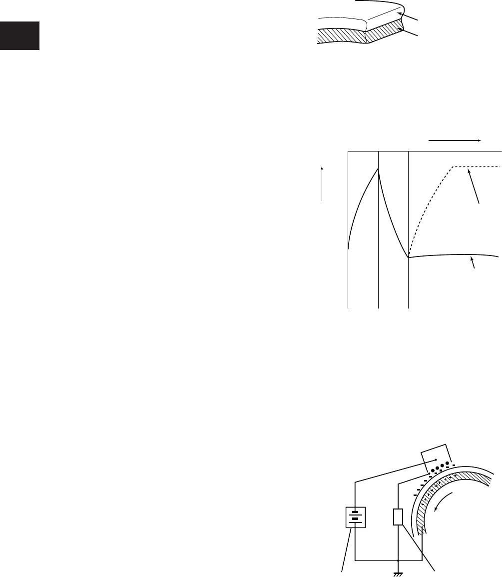
Charging is the process to apply charge evenly
on the drum surface.
The charger wire produces negative corona
discharge is controlled by the grid, allowing the
drum surface to be evenly charged with the
negative potential.
The surface potential on the drum is
determined by the grid potential and is
controlled to a certain value by the grid control
circuit.
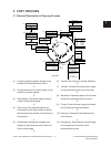
Photoconductive layer
Base
Structure of the photoconductive drum
(Example of OPC)
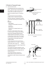
Main charger
Drum rotation
Grid control circuitHigh-voltage
transformer
Fig. 3-201
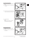
Fig. 3-203
0
– 500
– 1000
Time (t)
Black area of original
White area of original
Surface potential (V)
Discharge
process
Charging
process
Electric potential of the photoconductive drum
Fig. 3-202
04/01