


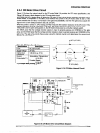
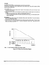
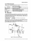
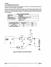
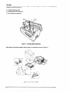
2.3.8 Plunger Drive Circuit
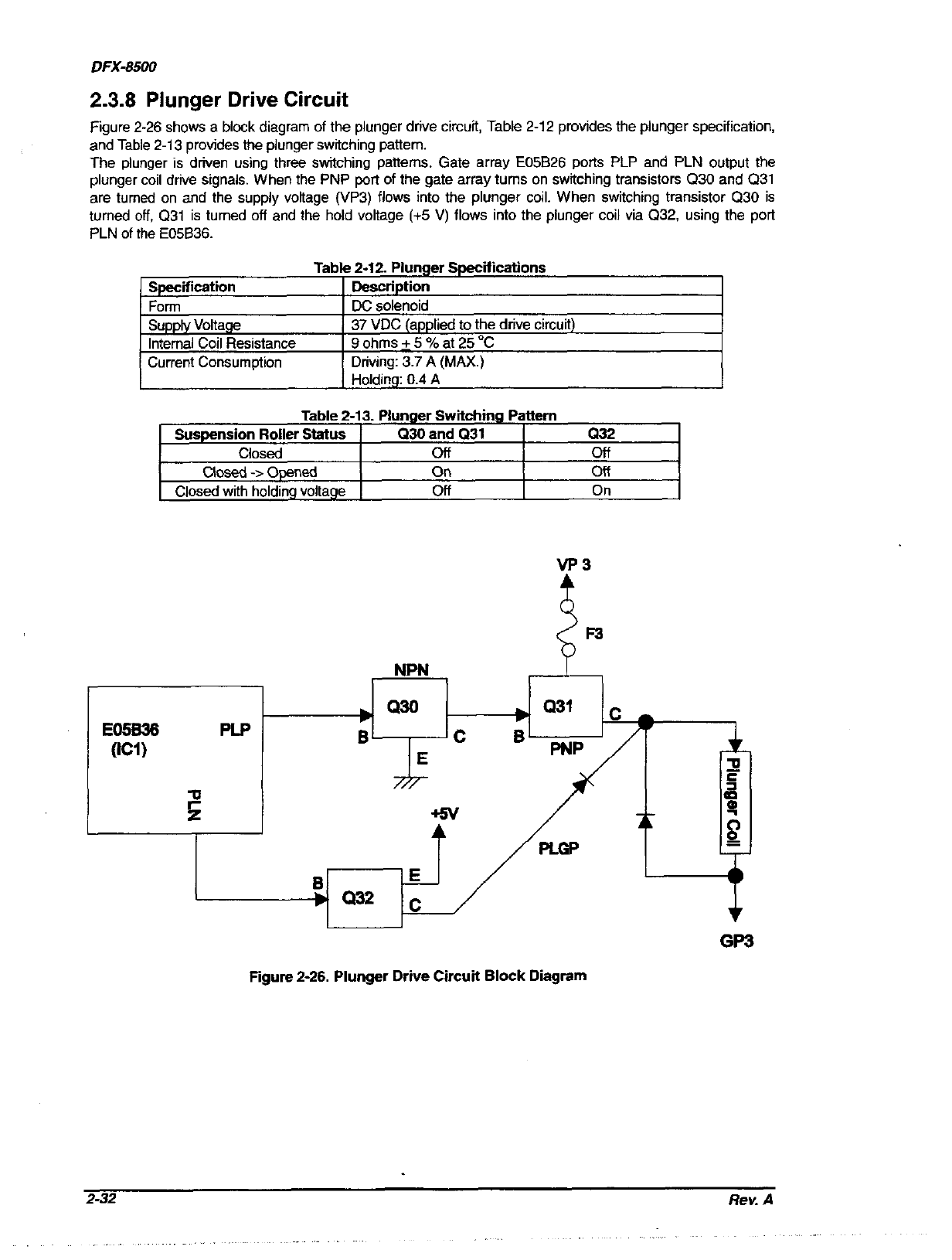
Figure 2-26 shows a block diagram of the plunger drive circuit, Table 2-12 provides the plunger specification,
and Table 2-13 provides the plunger switching pattern.
The plunger is driven using three switching patterns. Gate array E05826 ports PLP and PLN output the
plunger coil drive signals. When the PNP port of the gate array turns on switching transistors 030 and Q31
are turned on and the supply voltage (VP3) flows into the plunger coil. When switching transistor Q30 is
turned off, Q31 is turned off and the hold voltage (+5 V) flows into the plunger coil via 032, using the port
PLN of the E05B36.
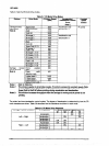
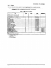
Table Z-12. Plunger Specifications
Specffication
Description
Form
DC solenoid
Suppfy Voltage 37 VDC (applied to the drive circuit)
Internal Coil Resistance 9ohms+5%at25’?
Current Consumption
Driving: 3.7 A (MAX.)
Holding: 0.4 A
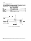
Table 2-13. Plunger Switching Pattern
Suspension Roller Status 1
om and m-41 I nw I
-_-__.- -_.
---
,
Closed
I
Off
I
Off
closed -> Opened
On
Qff
Closed with holding voftage 1 ofl
On
Figure 2-26. Plunger Drive Circuit Block Diagram