Chapter 4 Register Map and Descriptions
©
National Instruments Corporation 4-9 AT-MIO-16X User Manual
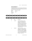
Command Register 2
Command Register 2 contains 15 bits that control AT-MIO-16X RTSI
bus transceivers, analog output configuration, and DMA Channels A
and B selection. Bits 8-15 of this register are cleared upon power up and
after a reset condition. Bits 0-7 of this register are undefined upon
power up and are not cleared after a reset condition. These bits should
be initialized through software.
Address: Base address + 02 (hex)
Type: Write-only
Word Size: 16-bit
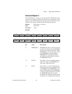
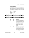
Bit Map:
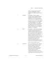
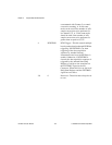
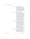
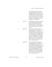
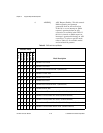
Bit Name Description
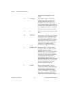
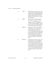
15 A4RCV RTSI A4 Receive—This bit controls the
signal source for the TMRTRIG* (Timer
Trigger) signal. The TMRTRIG* signal
updates the DACs in delayed update
mode. If A4RCV is set, pin A4 of the
RTSI switch drives the TMRTRIG*
signal. If A4RCV is cleared, the
TMRTRIG* signal is driven by the
EXTTMRTRG* signal from the I/O
connector.
14 A4DRV RTSI A4 Drive—This bit controls the
driver that allows the OUT5 signal to
drive pin A4 of the RTSI switch. If
A4DRV is set, pin A4 of the RTSI switch
is driven by OUT5. If A4DRV is cleared,
pin A4 is not driven by OUT5, and it can
be driven by a signal on the RTSI bus.
76 5
0
43
DMACHBB1
2
DMACHAB2
10
DMACHAB1EISA_DMA DMACHBB2 DMACHAB0DMACHBB0
15
MSB
LSB
14 13
A4DRV
12 11
A2DRV
10
BIPDAC0
98
EXTREFDAC1A4RCV A2RCV EXTREFDAC0BIPDAC1


