Chapter 4 Register Map and Descriptions
AT-MIO-16X User Manual 4-10
©
National Instruments Corporation
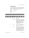
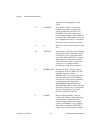
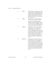
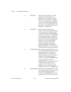
13 A2RCV RTSI A2 Receive—This bit controls the
driver that allows the GATE1 signal to be
driven from pin A2 of the RTSI switch. If
A2RCV is set, pin A2 of the RTSI switch
drives the GATE1 signal. In this case,
GATE1 may not be driven by a signal at
the I/O connector.
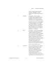
12 A2DRV RTSI A2 Drive—This bit controls the
driver that allows the OUT2 signal to
drive pin A2 of the RTSI switch. If
A2DRV is set, pin A2 of the RTSI switch
is driven by OUT2. If A2DRV is cleared,
pin A2 is not driven by OUT2, and it can
be driven by a signal on the RTSI bus.
11 BIPDAC1 Bipolar DAC 1—This bit configures the
range of DAC 1 in the analog output
section. If this bit is set, DAC 1 is
configured for bipolar operation of –V
ref
to +V
ref
. In this mode, data written to this
DAC is interpreted in two’s complement
format. If this bit is cleared, DAC 1 is
configured for unipolar operation of 0 V
to +V
ref
. In this mode, data written to
DAC 1 is interpreted in straight binary
format.
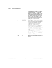
10 BIPDAC0 Bipolar DAC 0—This bit configures the
range of DAC 0 in the analog output
section. If this bit is set, then DAC 0 is
configured for bipolar operation of –V
ref
to +V
ref
. In this mode, data written to this
DAC is interpreted in two’s complement
format. If this bit is cleared, then DAC 0
is configured for unipolar operation of 0
V to +V
ref
. In this mode, data written to
DAC 0 is interpreted in straight binary
format.


