Chapter 2 Configuration and Installation
©
National Instruments Corporation 2-25 AT-MIO-16X User Manual
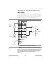
connect the negative side of the signal to AI GND as well as to the
negative (–) input of the PGIA. This works well for DC-coupled sources
with low source impedance (less than 100 Ω). However, for larger
source impedances, this connection leaves the differential signal path
significantly out of balance. Noise that couples electrostatically onto
the positive (+) line does not couple onto the negative (–) line because
it is connected to ground. Hence, this noise appears as a
differential-mode signal instead of a common-mode signal, and so the
PGIA does not reject it. In this case, instead of directly connecting the
negative (–) line to AI GND, connect it to AI GND through a resistor
that is about 100 times the equivalent source impedance. This puts the
signal path nearly in balance, so about the same noise couples onto both
(+) and (–) connections, yielding better rejection of electrostatically
coupled noise. Also, this configuration does not load down the source
(other than the 100-GΩ input impedance of the PGIA). You can fully
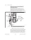
balance the signal path by connecting another resistor of the same value
between the positive (+) input and AI GND. This fully balanced
configuration offers slightly better noise rejection, but has the
disadvantage of loading the source down with the series combination
(sum) of the two resistors. If, for instance, the source impedance is 2 kΩ
and the two resistors are each 100 kΩ, the resistors load down the
source with 200 kΩ and produce a –1% gain error.
Both inputs of the PGIA require a DC path to ground in order for the
PGIA to work. If the source is AC coupled (capacitively coupled), then
the PGIA needs a resistor between the positive (+) input and AI GND.
If the source has low impedance, choose a resistor that is large enough
not to significantly load the source, but small enough not to produce
significant input offset voltage as a result of input bias current (typically
100 kΩ to 1 MΩ). If the source has high output impedance, you should
balance the signal path (as described above) using the same value
resistor on both the positive (+) and negative (–) inputs, and you should
be aware that there is some gain error from loading down the source.
The PGIA obtains its input DC bias currents from the DC paths to
ground. These currents are typically less than ±1 nA, but they contribute
significantly to error whenever the source has more than 1 kΩ
impedance or is AC coupled. If the source is DC coupled, the resulting
DC offset is less than 1 nA times the DC source resistance. For instance,
a 1-kΩ source will produce no more than 1 µV of input offset (0.33 LSB
at a gain of 100, bipolar range). If the source is AC coupled, then the
resulting DC offset is less than 1 nA times the sum of the two bias


