Chapter 3 Theory of Operation
©
National Instruments Corporation 3-3 AT-MIO-16X User Manual
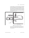
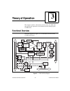
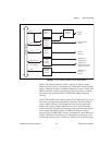
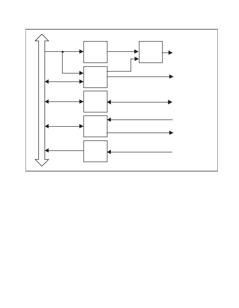
Figure 3-2. PC I/O Channel Interface Circuitry Block Diagram
The PC I/O channel interface circuitry consists of address latches,
address decoder circuitry, data buffers, PC I/O channel interface timing
signals, interrupt circuitry, and DMA arbitration circuitry. The PC I/O
channel interface circuitry generates the signals necessary to control
and monitor the operation of the AT-MIO-16X multiple-function
circuitry.
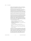
The PC I/O channel has 24 address lines; the AT-MIO-16X uses 10 of
these lines to decode the board address. Therefore, the board address
range is 000 to 3FF hex. SA5 through SA9 are used to generate the
board enable signal. SA0 through SA4 are used to select individual
onboard registers. The address-decoding circuitry generates the register
select signals that identify which AT-MIO-16X register is being
accessed. The AT-MIO-16X is factory configured for a base address of
220 hex. With this base address, all of the registers on the board will
fall into the address range of 220 hex to 23F hex. If this address range
PC I/O Channel
PC I/O
Channel
Timing
Interface
Address
Latches
Data
Buffers
DMA
Control
Circuitry
Interrupt
Control
Circuitry
Address
Decoder
Register
Selects
Read-and-Write
Signals
Internal
Data Bus
AT-MIO-16X
DMA Request
AT-MIO-16X
DMA Acknowledge
and Terminal Count
AT-MIO-16X
Interrupt
Request
Address
I/O Channel
Control Lines
16
/
DMA Request
IRQ
Bus
Data
Bus
DMA
Acknowledge


