Chapter 4 Register Map and Descriptions
©
National Instruments Corporation 4-3 AT-MIO-16X User Manual
Register Sizes
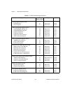
Two different transfer sizes for read-and-write operations are available
on the PC: byte (8-bit) and word (16-bit). Table 4-1 shows the size of
each AT-MIO-16X register. For example, reading the ADC FIFO
Register requires a 16-bit (word) read operation at the selected address,
whereas writing to the RTSI Strobe Register requires an 8-bit (byte)
write operation at the selected address. These register size accesses
must be adhered to for proper board operation. Performing a byte access
on a word location is an invalid operation and should be avoided. The
converse is also true. Performing a word access on a byte location is
also an invalid operation and should be avoided. You should pay
particular attention to the register sizes—they are very important.
Register Description Format
The remainder of this register description chapter discusses each of the
AT-MIO-16X registers in the order shown in Table 4-1. Each register
group is introduced, followed by a detailed bit description of each
register. The individual register description gives the address, type,
word size, and bit map of the register, followed by a description of
each bit.
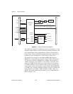
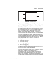
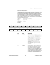
The register bit map shows a diagram of the register with the MSB
shown on the left (bit 15 for a 16-bit register, bit 7 for an 8-bit register),
and the LSB shown on the right (bit 0). A square is used to represent
each bit. Each bit is labeled with a name inside its square. An asterisk
(*) after the bit name indicates that the bit is inverted (negative logic).
In many of the registers, several bits are labeled with an X, indicating
don’t care bits. When a register is read, these bits may appear set or
cleared but should be ignored because they have no significance.
The bit map field for some registers states not applicable, no bits used.
Accessing these registers generates a strobe in the AT-MIO-16X. These
strobes are used to initiate some onboard event to occur. For example,
they can be used to clear the analog input circuitry or to start a data
acquisition operation. The data is ignored when writing to these
registers; therefore, any bit pattern suffices. Likewise, data returned
from a strobe register read access is meaningless.


