Chapter 3 Theory of Operation
©
National Instruments Corporation 3-29 AT-MIO-16X User Manual
Counter 5 is sometimes used by the data acquisition timing circuitry
and concatenated with Counter 4 to form a 32-bit sample counter.
The SCANCLK signal is connected to the SOURCE3 input of the
Am9513A, and OUT1 is sent to the data acquisition timing circuitry.
This allows Counter 1 to be used to divide the SCANCLK signal for
generating the CONFIGCLK signal. See the Data Acquisition Timing
Circuitry section earlier in this chapter.
Counter 2 is sometimes used by the data acquisition timing circuitry
to assign a time interval to each cycle through the scan sequence
programmed in the channel configuration register. This mode is called
interval channel scanning. See the Multiple-Channel Data Acquisition
section earlier in this chapter.
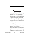
The Am9513A 4-bit programmable frequency output channel is located
at the I/O connector FOUT pin. Any of the five internal timebases and
any of the counter SOURCE or GATE inputs can be selected as the
frequency output source. The frequency output channel divides the
selected source by its 4-bit programmed value and makes the divided
down signal available at the FOUT pin.
RTSI Bus Interface Circuitry
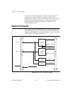
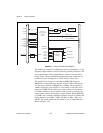
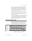
The AT-MIO-16X is interfaced to the National Instruments RTSI bus.
The RTSI bus has seven trigger lines and a system clock line. All
National Instruments AT Series boards with RTSI bus connectors can
be wired together inside the PC and share these signals. A block
diagram of the RTSI bus interface circuitry is shown in Figure 3-19.
Figure 3-19.
RTSI Bus Interface Circuitry Block Diagram
Trigger*
DAQPROG
DAQCMPLT
DAQCLEAR*
Interrupt
0120120
Channel
SCANCLK
CONVERT


