Chapter 5 Programming
©
National Instruments Corporation 5-39 AT-MIO-16X User Manual
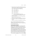
Note: If both the A2DRV and A2RCV bits are set, the GATE1 signal is driven by
the signal OUT2. This arrangement is probably not desirable.
• To drive the RTSI switch pin A4 with the signal OUT5, set
the A4DRV bit in Command Register 2. Otherwise, clear the
A4DRV bit.
• To drive the signal TMRTRIG* from pin A4 of the RTSI switch,
set the A4RCV bit in Command Register 2. Otherwise, clear the
A4RCV bit.
Note: If both the A4DRV and A4RCV bits are set, the TMRTRIG* signal is driven
by the signal OUT5.
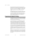
Programming the RTSI Switch
The RTSI switch is a 7×7 crossbar switch which can be programmed to
connect any of the signals on the A side to any of the signals on the
B side and vice versa. To do this, a 56-bit pattern is shifted into the
RTSI switch by writing one bit at a time to the RTSI Switch Shift
Register and then writing to the RTSI Switch Strobe Register to load the
pattern into the RTSI switch.
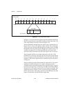
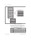
The 56-bit pattern is made up of two 28-bit patterns, one for side A and
one for side B of the RTSI switch. The low-order 28 bits select the
signal sources for the B-side pins. The high-order 28 bits select the
signal sources for the A-side pins. Each of the 28-bit patterns are made
up of seven 4-bit fields, one for each pin. The 4-bit field selects the
signal source and the output enable for the pin. Figure 5-10 shows the
bit map of the RTSI switch 56-bit pattern.


