Appendix A Specifications
©
National Instruments Corporation A-7 AT-MIO-16X User Manual
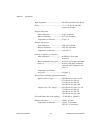
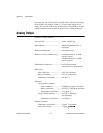
Output voltage ranges .........................0 to 10 V, unipolar mode;
±10 V, bipolar mode,
(software-selectable)
Current drive capability ......................±5 mA (short-circuit protected)
2 kΩ minimum load, 1,000 pF
maximum capacitive load
Output settling time to
±0.003% FSR......................................10 µsec for a 20 V step
Output slew rate..................................5 V/µsec
Output noise .......................................50 µV rms, DC to 1 MHz
Output impedance...............................0.3 Ω
External reference input impedance ....10 kΩ
External reference input range ............±18 V (protected to ±30 V,
power on or off)
External reference bandwidth
(–3 dB) ...............................................DC to 300 kHz
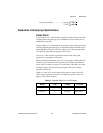
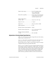
Explanation of Analog Output Specifications
Offset error is the amount of possible voltage offset error in the analog
output circuitry, expressed in mV.
Gain error is the amount of possible deviation from ideal gain of the
analog output circuitry, expressed as a proportion of the gain.
The total linear error for a DAC at a given output voltage is the output
voltage times the gain error, plus the offset error.
Relative accuracy in a DAC is the same as integral nonlinearity because
no uncertainty is added by quantization. Unlike an ADC, every digital
code in a DAC represents a specific analog value rather than a range of
values. The relative accuracy of the system is therefore limited to the
worst-case deviation from the ideal correspondence (a straight line),
excepting noise. If a DAC has been perfectly calibrated, then the
relative accuracy specification reflects its worst-case absolute error.


