Chapter 6 Calibration Procedures
©
National Instruments Corporation 6-9 AT-MIO-16X User Manual
a two's complement binary number in the onboard EEPROM for
subsequent use by the analog input calibration routines.
Because the onboard reference is very stable with respect to time and
temperature, it is seldom necessary to use the reference calibration
routine. Every year should be sufficient, or whenever operating the
board at an ambient temperature that is more than 10° C from the
temperature at which the reference value was last determined. Factory
calibration is performed at approximately 25° C.
Analog Input Calibration
To null out error sources that compromise the quality of measurements,
the input calibration routine calibrates the analog input circuitry by
adjusting the following potential sources of error:
• Pregain offset (offset error at the input of the PGIA)
• Postgain offset (offset error at the input of the ADC)
• Gain error of the analog input circuitry
Pregain offset contributes gain-dependent error to the analog input
system. This offset is multiplied by the gain of the PGIA. To calibrate
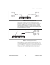
this offset, the routine grounds the inputs of the PGIA, measures the
input at two different gains, and adjusts CALDAC8 until the measured
offset in LSBs is independent of the gain setting.
Postgain offset is the total of the voltage offsets contributed by the
circuitry from the output of the PGIA to the ADC input (including the
ADC’s own offsets). To calibrate this offset, the routine grounds the
inputs of the PGIA and adjusts CALDAC2 and CALDAC3 until the
offset is within a small fraction of an LSB. The postgain offset is always
calibrated immediately after the pregain offset is calibrated.
If the three offset DACs are adjusted in this way, there is no significant
residual offset error, and reading a grounded channel returns (on
average) less than ±0.5 LSB, regardless of gain setting.
All the stages up to and including the input of the ADC contribute to the
gain error of the analog input circuitry. With the PGIA set to a gain of
1, the gain of the analog input circuitry is ideally 1. The gain error is the
deviation of the gain from 1 and appears as a multiplication of the input
voltage being measured. To eliminate this error source, the routine
measures the internal voltage reference and adjusts CALDAC0 and


