AMD Geode™ LX Processors Data Book 231
GeodeLink™ Memory Controller Register Descriptions
33234H
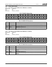
6.2.2.11 Feature Enables (MC_CF1017_DATA)
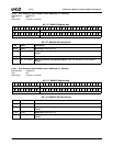
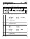
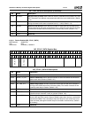
11:8 ACT2ACT ACT(0) to ACT(1) Period. tRRD. Minimum number of SDRAM clocks between ACT and
ACT command to two different component banks within the same module bank. (Default
= 7h)
7:6 DPLWR Data-in to PRE Period. tDPLW. Minimum number of clocks from last write data to pre-
charge command on the same component bank. (3..1 valid). Default = 10)
5:4 DPLRD Data-in to PRE Period. tDPLR. Minimum number of clocks from last read data to pre-
charge command on the same component bank.(3..1 valid) The count starts on the same
clock that the last data would have been if the command was a write. (Default = 10)
3 RSVD Reserved.
2:0 RSVD Reserved.
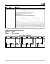
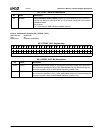
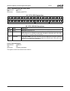
MSR Address 2000001Ah
Typ e R /W
Reset Value 00000000_11080001h
MC_CF8F_DATA Bit Descriptions (Continued)
Bit Name Description
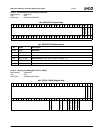
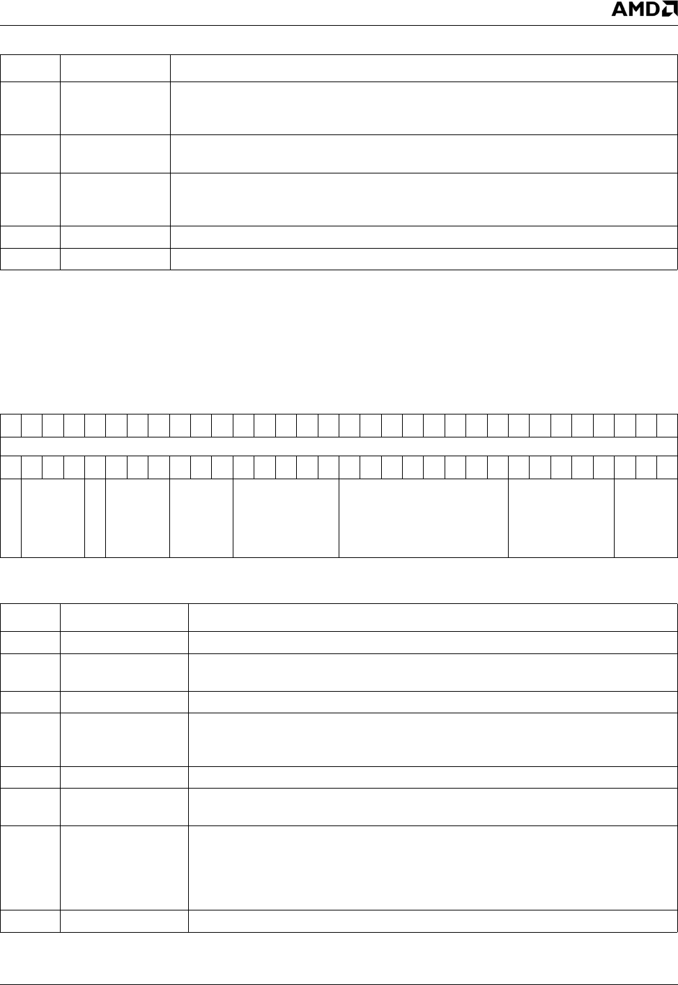
MC_CF1017_DATA Register Map
63 62 61 60 59 58 57 56 55 54 53 52 51 50 49 48 47 46 45 44 43 42 41 40 39 38 37 36 35 34 33 32
RSVD
31 30 29 28 27 26 25 24 23 22 21 20 19 18 17 16 15 14 13 12 11 10 9 8 7 6 5 4 3 2 1 0
RSVD
WR_TO_RD
RSVD
RD_TMG_CTL
RSVD REF2ACT PM1_UP_DLY RSVD WR2DAT
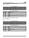
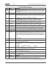
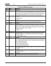
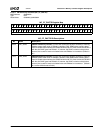
MC_CF1017_DATA Bit Descriptions
Bit Name Description
63:30 RSVD Reserved.
29:28 WRITE_TO_RD Write to Read Delay. tWTR. Minimum number of SDCLKS between last write data
beat to next read command. (Default = 01)
27 RSVD Reserved.
26:24 RD_TMG_CTL Read Timing Control. Number of half-GLIU clocks that the read data is delayed in
arriving at the GLMC beyond the CAS latency delay. This number increases as the
round-trip read delay increases. (Default = 001)
23:21 RSVD Reserved.
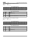
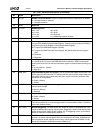
20:16 REF2ACT Refresh to Activate Delay. tRFC. Minimum number of SDCLKS (0-31) between
refresh and next command, usually an activate. (Default = 8h)
15:8 PM1_UP_DLY PMode1 Up Delay. Sets the delay in DRAM clocks from exit from PMode1 to accep-
tance of the next GLIU memory request. PMode1 power down involves a self-refresh
command to DRAM. This is to satisfy a 200-clock delay from self-refresh exit to first
read command (although this bit will delay all commands, read and write). (Default =
0, No delay)
7:3 RSVD Reserved.


