AMD Geode™ LX Processors Data Book 321
Display Controller Register Descriptions
33234H
6.6.4 Memory Organization Registers
The graphics memory region is up to 16 MB in size. The graphics memory is made up of the normal uncompressed frame
buffer, compressed display buffer, cursor buffer, cursor color buffer (for 16-bit color cursor), and video buffer(s). Each buffer
begins at a programmable offset within the graphics memory region.
The various memory buffers are arranged so as to efficiently pack the data within the graphics memory region. This
requires flexibility in the way that the buffers are arranged when different display modes are in use. The cursor and cursor
color buffers are linear blocks, so addressing is straightforward. The frame buffer and compressed display buffer are
arranged based upon scan lines. Each scan line has a maximum number of valid or active QWORDs and a pitch that, when
added to the previous line offset, points to the next line. In this way, the buffers may be stored as linear blocks or as rectan-
gular blocks.
The various buffers’ addresses are all located within the same 1 MB-aligned region. Thus, a separate register,
DC_GLIU0_MEM_OFFSET (DC Memory Offset 084h), is used to set a 1 MB-aligned base address.
GART address translation is not supported.
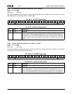
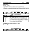
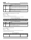
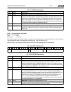
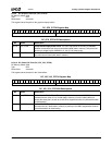
6.6.4.1 DC Frame Buffer Start Address (DC_FB_ST_OFFSET)
This register specifies the offset at which the frame buffer starts. Settings written to this register do not take effect until the
start of the following frame or interlaced field.
DC Memory Offset 010h
Typ e R /W
Reset Value xxxxxxxxh
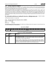
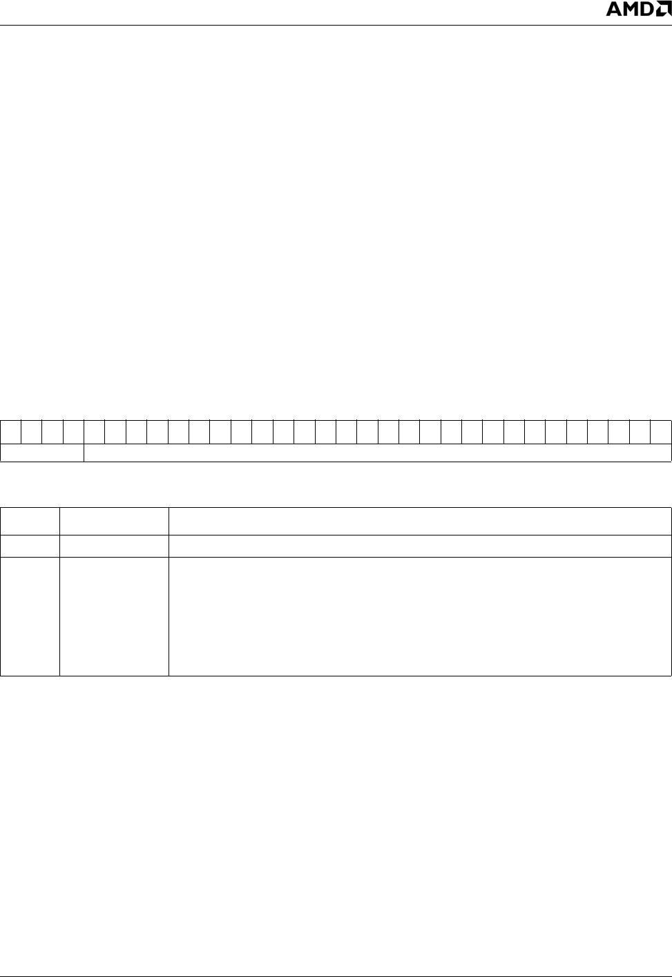
DC_FB_ST_OFFSET
313029282726252423222120191817161514131211109876543210
RSVD OFFSET
DC_FB_ST_OFFSET Bit Descriptions
Bit Name Description
31:28 RSVD Reserved.
27:0 OFFSET Frame Buffer Start Offset. This value represents the byte offset of the starting location
of the displayed frame buffer. This value may be changed to achieve panning across a
virtual desktop or to allow multiple buffering.
When this register is programmed to a non-zero value, the compression logic should be
disabled. The memory address defined by bits [27:3] takes effect at the start of the next
frame scan. The pixel offset defined by bits [2:0] is latched at the end of vertical sync and
added to the pixel panning offset to determine the actual panning value.


