AMD Geode™ LX Processors Data Book 95
CPU Core
33234H
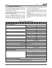
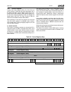
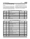
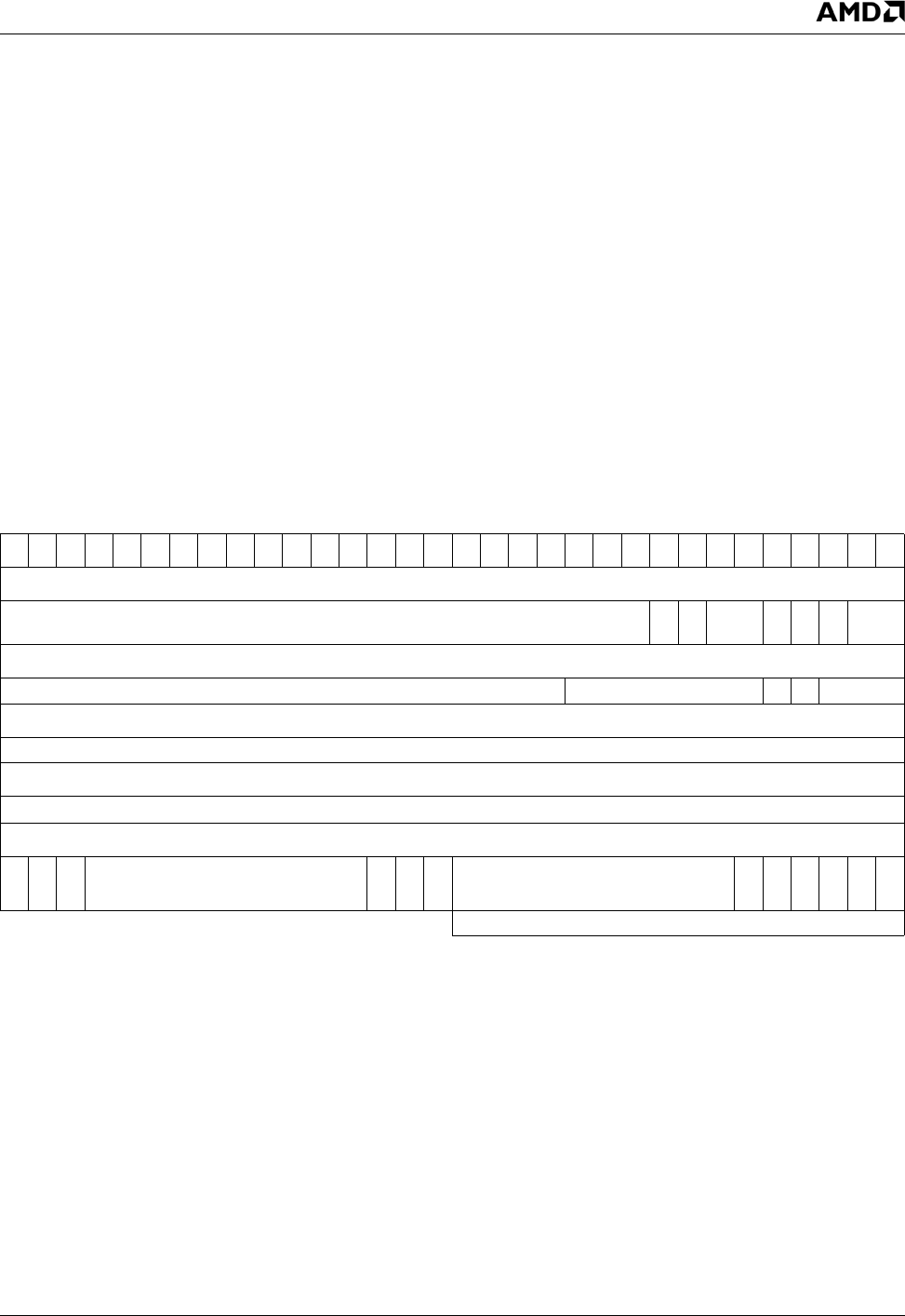
5.4.1 Control Registers
A map of the Control registers (CR0, CR1, CR2, CR3, and
CR4) is shown in Table 5-6 and the bit descriptions are in
the tables that follow. (These registers should not be con-
fused with the CRRn registers.) CR0 contains system con-
trol bits that configure operating modes and indicate the
general state of the CPU. The lower 16 bits of CR0 are
referred to as the Machine Status Word (MSW).
When operating in real mode, any program can read and
write the control registers. In protected mode, however,
only privilege level 0 (most-privileged) programs can read
and write these registers.
L1 Cache Controller
The Geode LX processor contains an on-board 64 KB L1
instruction cache, a 64 KB L1 write-back data cache, and a
128 KB unified L2 victim cache. With the memory controller
on-board, the L1 cache requires no external logic to main-
tain coherency. All DMA cycles automatically snoop the L1
and L2 caches.
The CD bit (Cache Disable, bit 30) in CR0 globally controls
the operating mode of the L1 and L2 caches. LCD and
LWT, Local Cache Disable and Local Write-through bits in
the Translation Lookaside Buffer, control the mode on a
page-by-page basis. Additionally, memory configuration
control can specify certain memory regions as non-cache-
able.
If the cache is disabled, no further cache line fills occur.
However, data already present in the cache continues to be
used. For the cache to be completely disabled, the cache
must be invalidated with a WBINVD instruction after the
cache has been disabled.
Write-back caching improves performance by relieving con-
gestion on slower external buses.
The Geode LX processor caches SMM regions, reducing
system management overhead to allow for hardware emu-
lation such as VGA.
Table 5-6. Control Registers Map
313029282726252423222120191817161514131211109876543210
CR4 Register Control Register 4 (R/W)
RSVD
PCE
PGE
RSVD
PSE
DE
TSC
RSVD
CR3 Register Control Register 3 (R/W)
PDBR (Page Directory Base Register) RSVD 0 0 RSVD
CR2 Register Control Register 2 (R/W)
PFLA (Page Fault Linear Address)
CR1 Register Control Register 1 (R/W)
RSVD
CR0 Register Control Register 0 (R/W)
PG
CD
NW
RSVD
AM
RSVD
WP
RSVD
NE
RSVD
TS
EM
MP
PE
Machine Status Word (MSW)


