428 AMD Geode™ LX Processors Data Book
Video Processor Register Descriptions
33234H
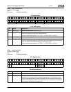
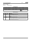
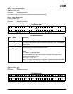
6.8.3.8 Palette Address (PAR)
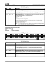
6.8.3.9 Palette Data (PDR)
VP Memory Offset 038h
Typ e R /W
Reset Value 00000000_000000xxh
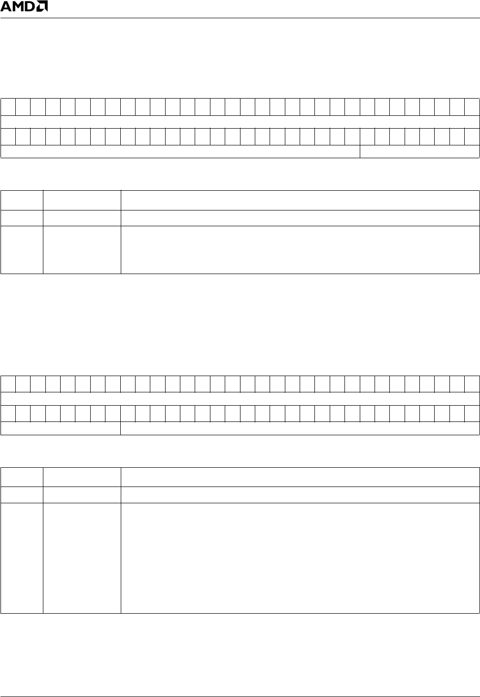
PAR Register Map
63 62 61 60 59 58 57 56 55 54 53 52 51 50 49 48 47 46 45 44 43 42 41 40 39 38 37 36 35 34 33 32
RSVD
313029282726252423222120191817161514131211109876543210
RSVD PAL_ADDR
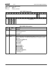
PAR Bit Descriptions
Bit Name Description
63:8 RSVD (RO) Reserved (Read Only). Reads back as 0.
7:0 PAL_ADDR Gamma Address. Specifies the address to be used for the next access to the Palette
Data register (VP Memory Offset 040h[23:0]). Each access to the PDR automatically
increments the PAR. If non-sequential access is made to the palette, the PAR must be
loaded between each non-sequential data block.
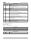
VP Memory Offset 040h
Typ e R /W
Reset Value 00000000_00xxxxxxh
PDR Register Map
63 62 61 60 59 58 57 56 55 54 53 52 51 50 49 48 47 46 45 44 43 42 41 40 39 38 37 36 35 34 33 32
RSVD
313029282726252423222120191817161514131211109876543210
RSVD PAL_DATA
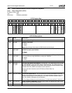
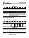
PDR Bit Descriptions
Bit Name Description
63:24 RSVD (RO) Reserved (Read Only). Reads back as 0.
23:0 PAL_DATA Palette Data. Contains the read or write data for a Gamma Correction RAM (palette).
Provides the video palette data. The data can be read or written to the Gamma Correc-
tion RAM (palette) via this register. Prior to accessing this register, an appropriate
address should be loaded to the PAR (VP Memory Offset 038h[7:0]). Subsequent
accesses to the PDR cause the internal address counter to be incremented for the next
cycle.
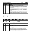
Note: When a read or write to the Gamma Correction RAM occurs, the previous output
value is held for one additional DOTCLK period. This effect should go unnoticed
during normal operation.


