AMD Geode™ LX Processors Data Book 285
Display Controller
33234H
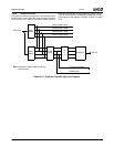
6.5.1.4 Display Refresh Compression
To reduce the system memory contention caused by the
display refresh, the GUI block contains compression and
decompression logic for compressing the frame buffer
image in real time as it is sent to the display. The DC does
not modify the standard frame buffer, but rather, it utilizes a
separate compressed display buffer for updating the dis-
play under certain conditions. This compressed display
buffer can be allocated within the extra off-screen memory
within the graphics memory region.
Coherency of the compressed display buffer is maintained
by use of dirty and valid bits for each line. Whenever a line
has been successfully compressed, it is retrieved from the
compressed display buffer for all future accesses until the
line becomes dirty again. Dirty lines are retrieved from the
normal uncompressed frame buffer.
The compression logic has the ability to insert a “static”
frame every other display frame, during which time dirty
bits are ignored and the valid bits are read to determine
whether a line should be retrieved from the frame buffer or
compressed display buffer. This allows a latency of one
frame between pixels actually being rendered and showing
up on the display. This effect typically goes unnoticed for
traditional 2D applications but may result in increased tear-
ing in single-buffered animation sequences. This feature
may be used to tune for maximum performance or optimal
display quality.
The compression algorithm used commonly achieves com-
pression ratios between 10:1 and 50:1, depending on the
nature of the display data. The compression algorithm
employed is lossless and therefore results in no loss of
visual quality. This high level of compression provides
higher system performance by reducing typical latency for
normal system memory access, higher graphics perfor-
mance by increasing available drawing bandwidth to the
memory subsystem, and lower power consumption by sig-
nificantly reducing the number of off-chip memory
accesses required for refreshing the display. These advan-
tages become more pronounced as display resolution,
color depth, and refresh rate are increased, and as the size
of the installed DRAM increases.
As uncompressed lines are fed to the display, they are
compressed and stored in an on-chip compressed line
buffer (64x64 bits). Lines will not be written back to the
compressed display buffer in the DRAM unless a success-
ful compression has resulted, so there is no penalty for
pathological frame buffer images where the compression
algorithm is sub-optimal.
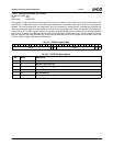
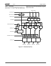
6.5.1.5 Dirty/Valid RAM
The DC module incorporates the Dirty/Valid RAM
(DVRAM) in the Display Controller module. The Dirty/Valid
RAM controller directly snoops GLIU0 request packets on
the memory data port.
The Dirty/Valid RAM may be used to monitor locations in
memory other than the frame buffer. (Compression and
decompression must be disabled in order for the Display
Controller to continue to function properly.) This may be
used for scenarios where software (or the Graphics Pro-
cessor) must modify or re-render a frame whenever corre-
sponding modifications occur in an offscreen graphics
buffer. The “palletized” bit is set upon writes to the corre-
sponding region of memory. However, it is up to software
to clear the dirty bit by writing to the Dirty/Valid RAM
Access register (DC Memory Offset 08Ch).
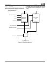
6.5.1.6 Palette/Gamma RAM
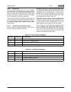
The GUI block contains a 261x24 color lookup table RAM
used for palletized display modes (Indexes 0-255), cursor
colors (Indexes 256-257), and the GUI mode border color
(Index 260). This color lookup table is also used by the
VGA block to map the 8-bit VGA pixels to a 24-bit RGB
color value. In true color display modes (16, 24, or 32-bpp),
the color lookup table can be used as a gamma correction
RAM.
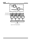
6.5.1.7 Display Address Generator
The GUI block supports flexible address generation for the
frame buffer, compressed display buffer, cursor and icon
buffers, and video buffers (YUV 4:2:2 or 4:2:0 format). A
separate start offset register is provided for each display
buffer. The start offset may be programmed to be relative
to frame buffer space (up to 256 MB).
6.5.1.8 Display Timing Generator
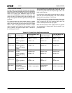
The GUI block includes a flexible timing generator capable
of handling up to a 1920x1440 resolution display. Horizon-
tal timings are programmable with 1-pixel granularity. Verti-
cal timings are programmable with scan line granularity.
The timing registers are master-slaved such that a new tim-
ing set may be programmed while the working set is still
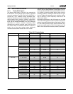
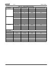
active. The TRUP configuration bit (DC_DISPLAY_CFG,
DC Memory Offset 008h[6]) is used to allow the new set of
timings to take effect at the start of vertical sync. As long as
the horizontal and vertical total counts do not change when
a new timing set is loaded, the sync pulses should remain
stable and the display should not glitch.


