AMD Geode™ LX Processors Data Book 519
Security Block Register Descriptions
33234H
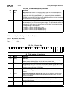
6.12.2 Security Block Specific MSRs
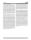
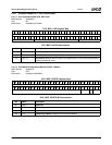
6.12.2.1 GLD Control MSR (GLD_MSR_CTRL)
MSR Address 58002006h
Typ e R /W
Reset Value 00000000_00000003h
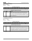
GLD_MSR_CTRL Register Map
63 62 61 60 59 58 57 56 55 54 53 52 51 50 49 48 47 46 45 44 43 42 41 40 39 38 37 36 35 34 33 32
RSVD
313029282726252423222120191817161514131211109876543210
RSVD
T_TM
T_NE
T_SEL
RSVD
TW
SBY
SBI
DIV
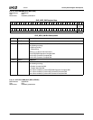
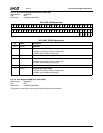
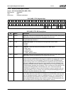
GLD_MSR_CTRL Bit Descriptions
Bit Name Description
63:12 RSVD Reserved. These bits are implemented but reserved for future use. When writing to this
MSR, software should set these bits to 0 and ignore them on read.
11 T_TM TRNG Test Mode. This bits enables the TRNG test mode. Deterministic TRNG values
are generated when this bit is 1.
10 T_NE TRNG Noise Enable. This bit enables the noise generator for the TRNG.
0: Disable.
1: Enable.
9:8 T_SEL TRNG SEL. These bits select post processing of the TRNG output.
00: Raw output.
01: LFSR output.
10: Whitener output.
11: LFSR + Whitener output.
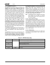
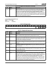
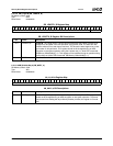
7:5 RSVD Reserved. These bits are implemented but reserved for future use. When writing to this
MSR, software should set these bits to 0 and ignore them on read.
4TW Time Write. This bit controls the EEPROM write timing within the EEPROM interface
module. Normally the EEPROM interface signals completion immediately after it finishes
shifting out the last bit of a write operation. The start of any other EEPROM access
begins a polling process. Once, the EEPROM has completed its internally timed write
operation, it responds to the polling and the next operation can begin. Setting this bit
causes the EEPROM interface to delay for slightly more than 10 ms after writing to the
EEPROM, before indicating write completion. That is, the start bit will be held high, and
the interrupt and SMI generation will be delayed for 10 ms. This ensures that the
EEPROM has completed its internal write and should be ready to respond to the next
access immediately. This is a “chicken” bit to avoid using the acknowledge polling (as
described in the Atmel datasheet), after a write.
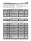
3 SBY Swap Bytes. This bit controls a byte-swapping feature within the AES module. When
set, the bytes within the 16-byte block are swapped on both AES DMA reads and writes.
Byte 15 is swapped with byte 0, byte 14 is swapped with byte 1, etc. Asserting this bit
does not affect the slave operations to AES registers, (including the writable key), nor
does it affect EEPROM operations. When this bit is cleared, the DMA operations read
and write bytes with the same byte order as they appear in memory.


