332 AMD Geode™ LX Processors Data Book
Display Controller Register Descriptions
33234H
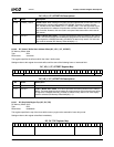
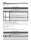
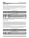
6.6.5.7 DC Frame Buffer Active Region Register (DC_FB_ACTIVE)
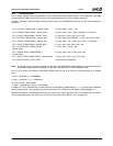
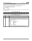
6.6.6 Cursor Position and Line Count/Status Registers
The cursor registers contain pixel coordinate information for the cursor. These values are not latched by the timing genera-
tor until the start of the frame to avoid tearing artifacts when moving the cursor.
The Line Count/Status register holds status information for the current display status, including the current scan line for the
display.
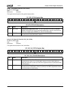
6.6.6.1 DC Cursor X Position (DC_CURSOR_X)
This register contains the X position information of the hardware cursor.
Settings written to this register do not take effect until the start of the following frame or interlaced field.
DC Memory Offset 05Ch
Typ e R /W
Reset Value xxxxxxxxh
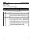
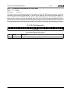
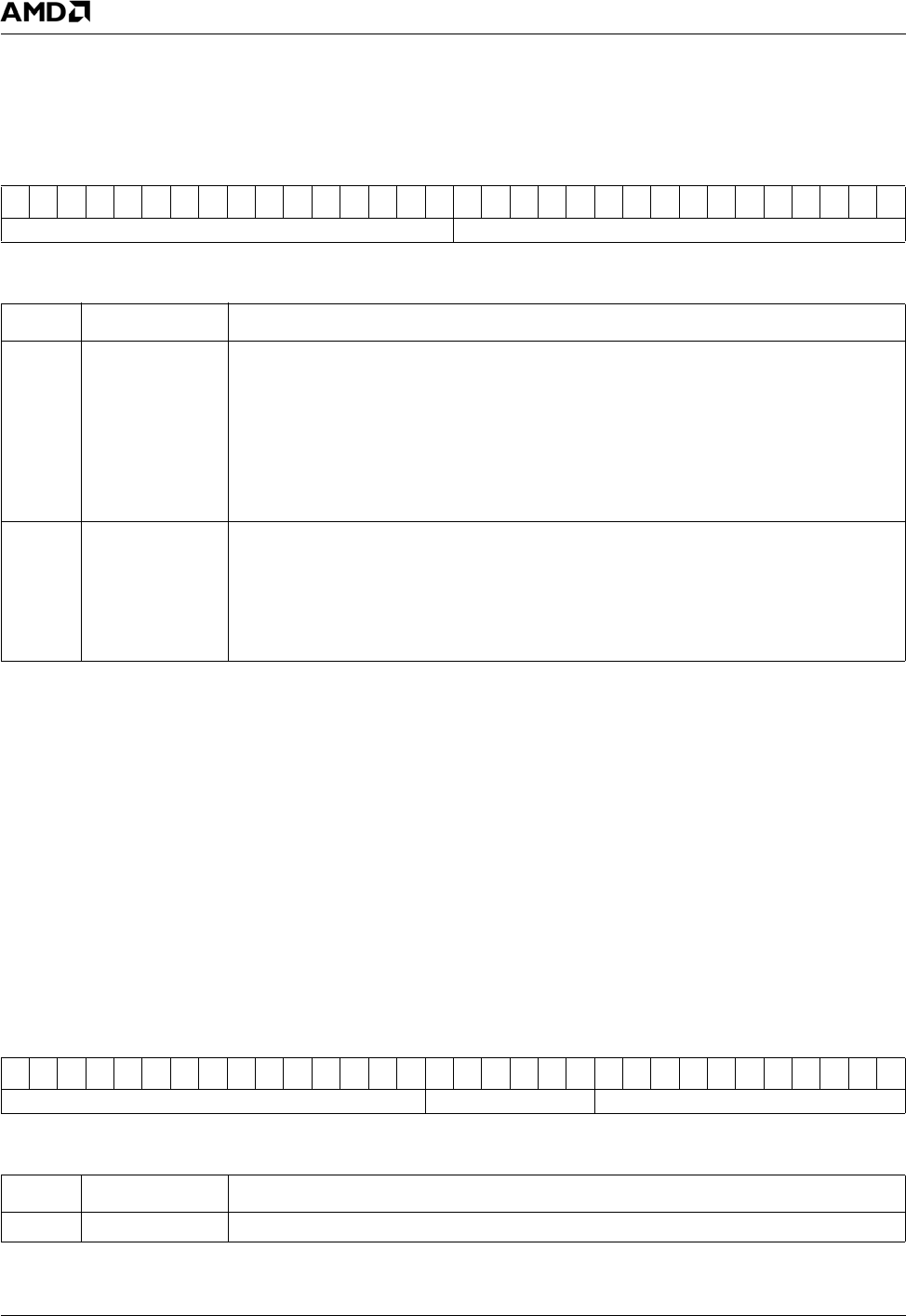
DC_FB_ACTIVE Register Map
313029282726252423222120191817161514131211109876543210
FB_H_ACTIVE FB_V_ACTIVE
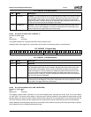
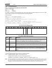
DC_FB_ACTIVE Bit Descriptions
Bit Name Description
31:16 FB_H_ACTIVE Horizontal Frame Buffer Active End. This field is used only when graphics scaling is
enabled. The lower three bits of this register are ignored and presumed to be 111. Includ-
ing these bits, the value in this field represents the total number of pixels in a line in the
graphics frame buffer minus 1.
This field is analogous to the H_ACTIVE field in the DC_H_ACTIVE_TIMING register
(DC Memory Offset 040h[11:0]), except that this field is used only for the fetching and
rendering of pixel data, not the display timings. When graphics scaling is disabled, this
field is not used. (The H_ACTIVE field is used instead.
15:0 FB_V_ACTIVE Vertical Frame Buffer Active. This field is used only when graphics scaling is enabled.
It represents the total number of lines in the graphics frame buffer minus 1.
This field is analogous to the V_ACTIVE field in the DC_V_ACTIVE_TIMING register (DC
Memory Offset 050h[10:0]), except that this field is used only for the fetching and render-
ing of pixel data, not the display timings. When graphics scaling is disabled, this field is
not used. (The V_ACTIVE field is used instead.)
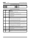
DC Memory Offset 060h
Typ e R /W
Reset Value xxxxxxxxh
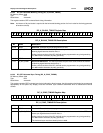
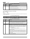
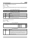
DC_CURSOR_X Register Map
313029282726252423222120191817161514131211109876543210
RSVD X_OFFSET CURSOR_X
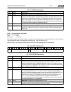
DC_CURSOR_X Bit Descriptions
Bit Name Description
31:17 RSVD Reserved.


