AMD Geode™ LX Processors Data Book 569
GeodeLink™ PCI Bridge
33234H
6.15.4 PCI Bus Interface Block
The PCI Bus Interface block is compliant to the PCI 2.2
specification, except in the handling of SERR#/PERR# sig-
nals. These signals are not available.
The PCI Bus Interface block provides a protocol conversion
layer between the Transaction Forwarding block and the
PCI bus. The master and target portions of this block oper-
ate independently. Thus, out-bound write requests and in-
bound read responses are effectively multiplexed onto the
PCI bus. It generates configuration cycles and software
generated special cycles using the standard 0CF8h/0CFCh
I/O address scheme. It includes address decoding logic to
recognize distinct address regions for slave operation.
Each address region is defined by a base address, a size,
and some attached attributes (i.e., prefetchable, coherent).
This block is responsible for retrying out-bound requests
when a slave termination without data is seen on the PCI
bus. It must restart transactions on the PCI bus that are
prematurely ended with a slave termination. This block
always slave terminates in-bound read transactions issued
to non-prefetchable regions after a single DWORD has
been transferred.
The maximum inbound write throughput is only limited by
the PCI latency timer (see register GLPCI_CTRL bits
[39:35]), which will interrupt an inbound transaction after
the specified number of cycles. With this latency timer dis-
abled (GLPCI_CTRL bit 9), the maximum throughput is
achieved
The maximum inbound read throughput is also affected by
the PCI latency timer in a similar fashion to the inbound
write throughput. It is also affected by the inbound read
prefetch threshold setting (GLPCI_CTRL bits [59:56]). With
the latency timer disabled and the read prefetch set to 0Ah
to 0Fh, the maximum throughput is achieved. With the read
prefetch threshold set to the default of 04h, the throughput
is not optimal.
6.15.4.1 PCI Configuration and Virtual PCI Header
Support
The PCI Bus Interface block implements the logic to gener-
ate PCI configuration cycles. The standard mechanism for
generating PCI configuration cycles (as described in the
PCI 2.2 specification) is used.
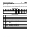
To access the internal PCI configuration registers of the
AMD Geode LX processor, the Configuration Address reg-
ister (CONFIG_ADDRESS) must be written as a DWORD
using the format shown in Table 6-89. Any other size will be
interpreted as an I/O write to Port 0CF8h. Also, when
entering the Configuration Index, only the six most signifi-
cant bits of the offset are used, and the two least significant
bits must be 00.
BYTE and WORD sized I/O accesses to 0CF8h pass
through the PCI Bus Interface block onto the PCI bus.
Writes to the CONFIG_DATA register are translated into
PCI configuration write bus cycles. Reads to the
CONFIG_DATA register are translated into PCI configura-
tion read bus cycles. Bit 31 of the CONFIG_ADDRESS
register gates the translation of I/O accesses to 0CFCh into
PCI configuration cycles.
IDSEL assertions are realized where device numbers 1
through 21 are mapped to the AD[11] through AD[31] pins.
In addition, support is included for virtualization of PCI
buses and secondary bus devices. When a device or bus is
virtualized, the PCI Bus Interface block generates a syn-
chronous SMI for access to the CONFIG_DATA register
instead of generating a configuration cycle on the PCI bus.
See GLPCI_PBUS (MSR register (MSR 50002012h[31:0])
for details on virtual PCI header support.
The PCI Bus Interface block can be configured to accept
in-bound PCI configuration cycles. This is used as a debug
method for indirectly accessing the internal model specific
register from the PCI bus. When this capability is enabled,
the PCI Bus Interface block responds to in-bound PCI con-
figuration cycles that make the PCI Bus Interface block’s
IDSEL signal become asserted (expected to be device 1).
In this case, the PCI Bus Interface block ignores writes and
returns FFFFFFFFh for accesses to locations 00h through
EFh of the PCI configuration space. This makes the PCI
Bus Interface block invisible to PCI Plug&Play software.
Table 6-89. Format for Accessing the Internal PCI Configuration Registers
313029282726252423222120191817161514131211109876543210
1 Reserved 0000000000000000 Configuration Index 00


