5 - 16
Project name QB-12
Program name MAIN
5.2.2 BIN (P) BCD → BIN data conversion instruction
Operations to read and write data after step 35
S D
X7 T0
T0
T0
K50
C10
K1500
X0
D5
K4X2030 BINP
X0
D6
K4X2034 MOV
0
Check the difference
from the BIN instruction.
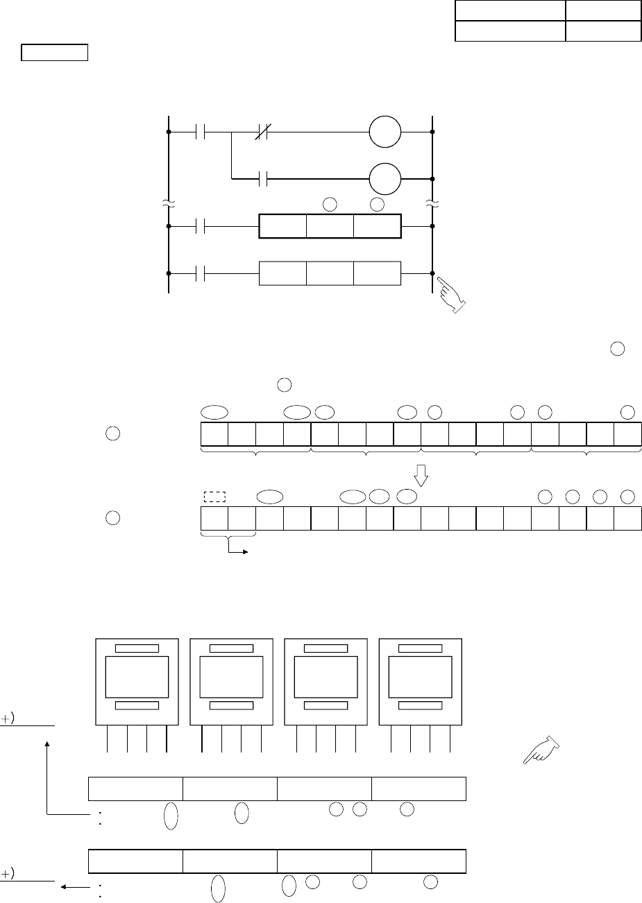
• When the input condition is turned on, the data in the device specified in
S
is
recognized as a BCD code, converted into binary (BIN code), and transferred to
the device specified in
D
.
1
9999
8000
4000 2000 1000
800
400 200 100 80 40 20 10 8 4 2 1
BCD
side
Thousand digits
0
0 1 1 0 0 1 1 0 0 1 1 0 0 1
Hundred digits Ten digits Unit digits
Converted into BIN
0
9999
163848192
4096 2048
1024 512
256
128 64 32
16
8421
BIN
side
Becomes 0.
0 1 0 0 1 1 1 0 0 0 0 1 1 1 1
D
S
• The ordinary digital switches generate BCD codes. Therefore, the BIN instruction
is required for writing data from the digital switches to the programmable
controller.
X2F
8
X2E
4
X2D
2
X2C
1)
1
X2B
8
X2A
4
X29
2)
X28
1
2
X27
8
X26
4
X25
X24
3
X23
8
X22
4)
X21
2
X20
1
4
Digital switch
4
16
32
512
4096
4660
0001001000110100
16384
8192
4096
2048
1024
512
256
128
64
32
16
8
4
2
1
D6
When the BCD code
is input without converted.
0000010011010010
16384
8192
4096
2048
1024
512
256
128
64
32
16
8
4
2
1
D5
When the BCD code is input after
converted into the binary code.
2
16
64
128
1024
1234
K4X20
1)2)


