


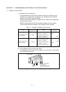
7 - 9
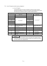
7.5.3 List of I/O signals and buffer memory assignment
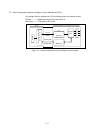
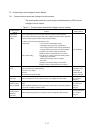
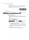
(1) List of I/O signals
The following shows a list of the I/O signals for the A/D converter modules.
Note that I/O numbers (X/Y) shown in this section and thereafter are the values
when the start I/O number for the A/D converter module is set to 0.
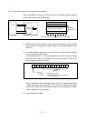
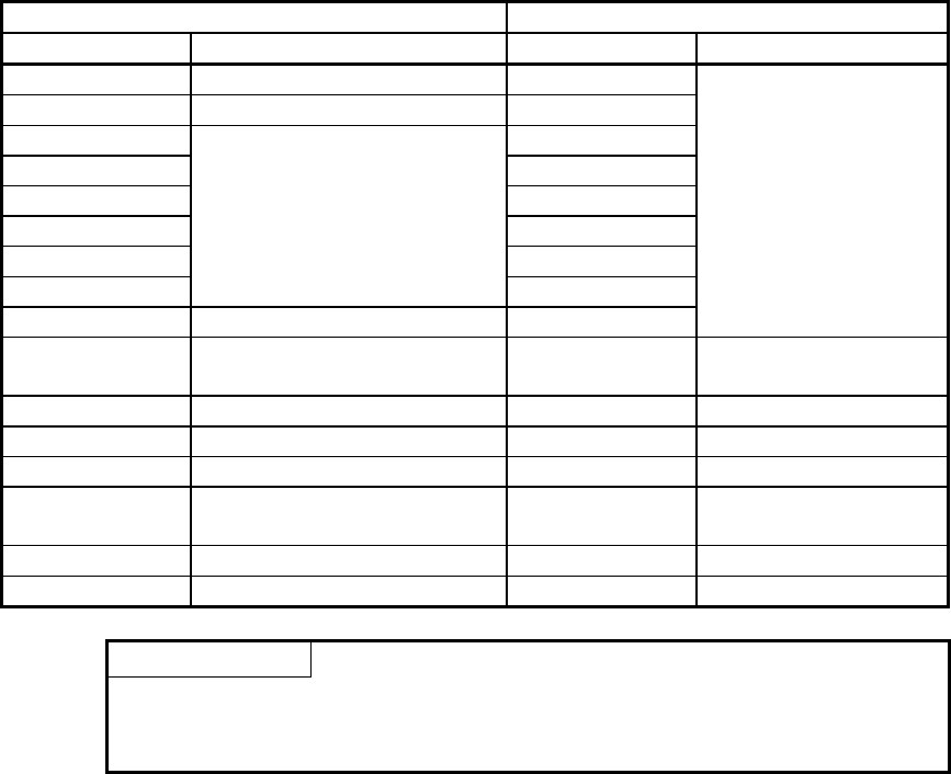
Signal direction: CPU ← A/D converter module Signal direction: CPU → A/D converter module
Device No. (input) Signal name Device No. (output) Signal name
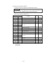
X0 Module READY Y0
X1 Temperature drift compensation flag Y1
X2 Y2
X3 Y3
X4 Y4
X5 Y5
X6 Y6
X7
Use prohibited
*1
Y7
X8 High resolution mode status flag Y8
Use prohibited
*1
X9
Operating condition setting
completed flag
Y9
Operating condition setting
request
XA Offset/gain setting mode flag YA User range writing request
XB Channel change completed flag YB Channel change request
XC Use prohibited
*1
YC Use prohibited
*1
XD
Maximum value/minimum value reset
completed flag
YD
Maximum value/minimum
value reset request
XE A/D conversion completed flag YE Use prohibited
*1
XF Error flag YF Error clear request
POINT
*1: These signals cannot be used by the user since they are for system use only.
If these are turned on/off by the sequence program, the functioning of the A/D
converter module cannot be guaranteed.