System Control Coprocessor
ARM DDI 0363E Copyright © 2009 ARM Limited. All rights reserved. 4-22
ID013010 Non-Confidential, Unrestricted Access
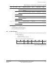
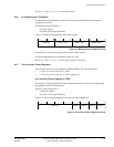
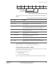
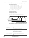
Figure 4-15 Memory Model Feature Register 0 format
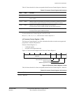
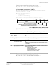
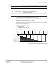
Table 4-10 shows how the bit values correspond with the Memory Model Feature Register 0
functions.
To access the Memory Model Feature Register 0 read CP15 with:
MRC p15, 0, <Rd>, c0, c1, 4 ; Read Memory Model Feature Register 0.
c0, Memory Model Feature Register 1, MMFR1
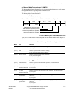
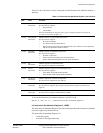
The Memory Model Feature Register 1 provides information about the memory model, memory
management, and cache support of the processor.
The Memory Model Feature Register 1 is:
• a read-only register
• accessible in Privileged mode only.
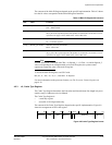
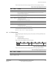
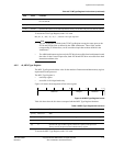
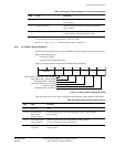
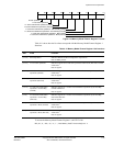
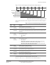
Figure 4-16 on page 4-23 shows the bit arrangement for Memory Model Feature Register 1.
31 28 27 24 23 20 19 16 15 12 11 8 7 4 3 0
Reserved FCSE TCM PMSA VMSA
Auxiliary Control Register
Cache coherence
Outer shareable
Table 4-10 Memory Model Feature Register 0 bit functions
Bits Field Function
[31:28] Reserved SBZ.
[27:24] FCSE Indicates support for Fast Context Switch Extension (FCSE).
0x0
, no support.
[23:20] Auxiliary Control Register Indicates support for the auxiliary registers.
0x2
, the processor supports the Auxiliary Instruction and Data Fault Status
Registers (AIFSR and ADFSR) and the Auxiliary Control Register.
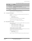
[19:16] TCM Indicates support for TCM and associated DMA.
0x1
, implementation defined.
[15:12] Outer shareable Indicates support for the Outer shareable attribute.
0x0
, no support.
[11:8] Cache coherence Indicates support for cache coherency maintenance.
0x0
, no support for shared caches.
[7:4] PMSA Indicates support for Physical Memory System Architecture (PMSA).
0x3
, the processor supports PMSAv7 (subsection support).
[3:0] VMSA Indicates support for Virtual Memory System Architecture (VMSA).
0x0
, no support.


