Level Two Interface
ARM DDI 0363E Copyright © 2009 ARM Limited. All rights reserved. 9-27
ID013010 Non-Confidential, Unrestricted Access
Note
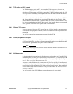
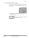
You can only access the cache RAMs using 32-bit or 64-bit AXI transfers. Using an 8-bit or a
16-bit transfer size generates a SLVERR error response.
Data RAM access
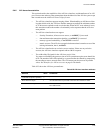
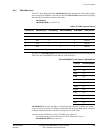
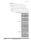
The following tables shows the data formats for cache data RAM accesses:
• Table 9-32 shows the format when neither parity nor ECC is implemented
• Table 9-33 on page 9-28 shows the format when parity is implemented
• Table 9-34 on page 9-28 shows the instruction cache format when ECC is implemented
• Table 9-35 on page 9-28 shows the data cache format when ECC is implemented.
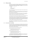
0010 Bank 1 1
0100 Bank 2 2
1000 Bank 3 3
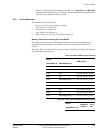
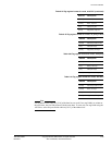
Table 9-31 Cache data RAM bank/address decode
Inputs
RAM bank
selected
ARADDRS[18:15] ARADDRS[3]
0001 0 Bank 0
0001 1 Bank 1
0010 0 Bank 2
0010 1 Bank 3
0100 0 Bank 4
0100 1 Bank 5
1000 0 Bank 6
1000 1 Bank 7
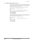
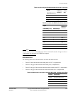
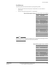
Table 9-32 Data format, instruction cache and data cache, no parity and no ECC
Data bit Description
[63:48] Not used, read-as-zero
[47:32] Data value, [31:16] or [63:48]
[31:16] Not used, read-as-zero
[15:0] Data value, [15:0] or [47:32]
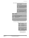
Table 9-30 Cache tag/valid RAM bank/address decode (continued)
Inputs
RAM bank
selected
Cache
way
ARADDRS[18:15]


