Level One Memory System
ARM DDI 0363E Copyright © 2009 ARM Limited. All rights reserved. 8-2
ID013010 Non-Confidential, Unrestricted Access
8.1 About the L1 memory system
The processor L1 memory system can be configured during implementation and integration. It
can consist of:
• separate instruction and data caches
• multiple Tightly-Coupled Memory (TCM) areas
•a Memory Protection Unit (MPU).
The instruction-side and data-side can each optionally have their own L1 caches. The cache
architecture is Harvard, that is, only instructions can be fetched from the i-cache, and only data
can be fetched from the d-cache. In parallel with each of the caches are two areas of dedicated
RAM accessible to both the instruction and data sides. These are regions of TCM. You can
implement one TCM using the ATCM interface and up to two TCMs using the BTCM interface.
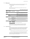
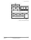
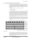
Figure 8-1 on page 8-3 shows this.
Each TCM and cache can be configured at implementation time to have an error detection and
correction scheme to protect the data stored in the memory from errors. Each TCM interface
also has support for logic external to the processor to tell the processor that an error has
occurred.
The MPU handles accesses to both the instruction and data sides. The MPU is responsible for
protection checking, address access permissions, and memory attributes. Some of these
functions can be passed to the L2 memory system through the AXI master. See Chapter 7
Memory Protection Unit for more information about the MPU.
The L1 memory system includes a monitor for exclusive accesses. Exclusive load and store
instructions can be used, for example,
LDREX
,
STREX
, with the appropriate memory monitoring to
provide inter-process or inter-processor synchronization and semaphores. See the ARM
Architecture Reference Manual for more details. The monitor can handle some exclusive
monitoring internally to the processor.


