Processor Signal Descriptions
ARM DDI 0363E Copyright © 2009 ARM Limited. All rights reserved. A-8
ID013010 Non-Confidential, Unrestricted Access
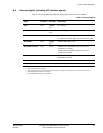
A.5 L2 interface signals
This section describes the processor L2 interface AXI signals. For more information on
Advanced Microcontroller Bus Architecture (AMBA) AXI signals see the AMBA AXI Protocol
Specification.
Note
All the outputs listed in this section have their reset values during standby.
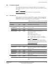
A.5.1 AXI master port
Table A-4 shows the AXI master port signals for the L2 interface. With the exception of the
ACLKENM, all signals are only sampled or driven on CLKIN edges when ACLKENM is
asserted, see AXI interface clocking on page 3-9 for more information.
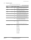
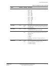
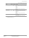
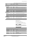
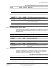
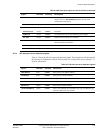
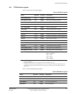
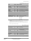
Table A-4 AXI master port signals for the L2 interface
Signal Direction Clocking Description
ACLKENM Input CLKIN Clock enable for the AXI master port.
Write address channel
AWADDRM[31:0] Output CLKIN Transfer start address.
AWBURSTM[1:0] Output CLKIN Write burst type.
AWCACHEM[3:0] Output CLKIN Provides decode information for outer attributes:
b0000 = Strongly Ordered.
b0001 = Device.
b0011 = Normal, Non-cacheable.
b0110 = Normal, Cacheable. write-through.
b1111 = Normal, Cacheable. write-back, write allocation.
b0111 = Normal, Cacheable. write-back, no write allocation.
Note
The AXI specification describes these encodings using the
pre-ARMv6 terms such as cacheable-bufferable. These terms
are equivalent to the ARMv6 memory-type descriptions such as
Normal, Non-cacheable used here.
AW IDM [3:0 ] Output CLKIN The identification tag for the write address group of signals.
AWLENM [3:0] Output CLKIN Write transfer burst length. The transfer burst length range is
from one to 16. A 4-bit binary value minus one determines the
transfer burst length.
AWLOCKM[1:0] Output CLKIN Lock signal.
AWPROTM[2:0] Output CLKIN Protection type. Only bit [0] is used from the 3-bit AXI bus.
AWREADYM Input CLKIN Address ready. The slave uses this signal to indicate that it can
accept the address.
AWSIZEM[2:0] Output CLKIN Indicates the size of the transfer.
AWUSERM[4:0] Output CLKIN Provides decode information for the write address channel. See
Table 9-3 on page 9-5 for information about the encoding of this
signal.


