


System Control Coprocessor
ARM DDI 0363E Copyright © 2009 ARM Limited. All rights reserved. 4-42
ID013010 Non-Confidential, Unrestricted Access
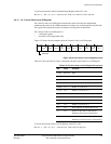
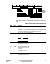
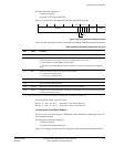
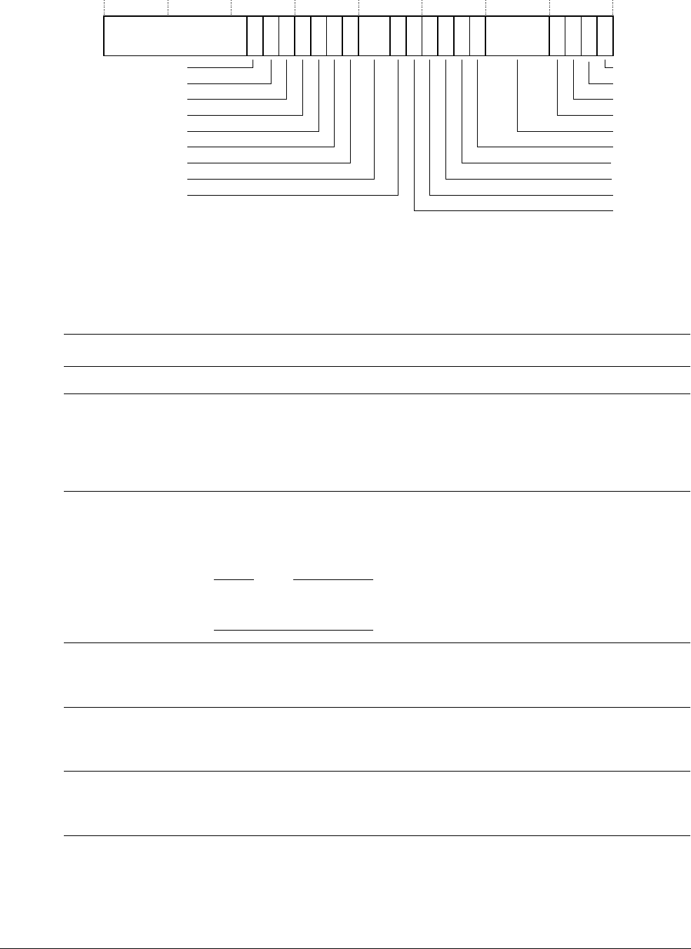
Figure 4-29 Secondary Auxiliary Control Register format
Table 4-25 shows how the bit values correspond with the Secondary Auxiliary Control Register
functions.
Reserved
31
22
21
19 18
17
16 15 14 13 12 11 7 3 2 1 01020 9 48
DR2B
DF6DI
DF2DI
DOODPFP
DDI
ATCMRMW
ATCMECC
IDC
DZC
IOC
UFC
OFC
IXC
DOOFMACS
BTCMRMW
B0TCMECC
Reserved
Reserved
DCHE
23
Table 4-25 Secondary Auxiliary Control Register bit functions
Bits Field Function
[31:23] Reserved SBZ.
[22] DCHE
Disable hard-error support in the caches.
a
0 = Enabled. The cache logic recovers from some hard errors. You must not use this value on
revisions r1p2 or earlier of the processor.
1 = Disabled. Most hard errors in the caches are fatal. This is the reset value.
See Hard errors on page 8-5 for more information.
[21]
DR2B
b
Enable random 2-bit error generation in cache RAMs. This bit has no effect unless ECC is
configured, see Configurable options on page 1-13.
0 = Disabled. This is the reset value.
1 = Enabled.
Note
This bit controls error generation logic during system validation. A synthesized ASIC
typically does not have such models and this bit is therefore redundant for ASICs.
[20] DF6DI
F6 dual issue control.
c
0 = Enabled. This is the reset value.
1 = Disabled.
[19] DF2DI
F2_Id/F2_st/F2D dual issue control.
c
0 = Enabled. This is the reset value.
1 = Disabled.
[18] DDI
F1/F3/F4dual issue control.
c
0 = Enabled. This is the reset value.
1 = Disabled.
[17] DOODPFP
Out-of-order Double Precision Floating Point instruction control.
c
0 = Enabled. This is the reset value.
1 = Disabled.