Processor Signal Descriptions
ARM DDI 0363E Copyright © 2009 ARM Limited. All rights reserved. A-12
ID013010 Non-Confidential, Unrestricted Access
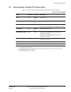
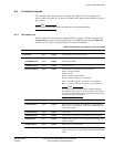
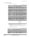
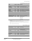
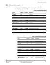
A.5.4 AXI slave port error detection signals
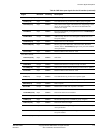
Table A-7 shows the AXI slave port error detection signals. These signals are only generated if
the processor is configured to include AXI bus parity. See Configurable options on page 1-13
for more information.
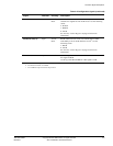
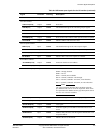
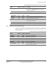
ARUSERS[3:0] Input CLKIN Memory type select {data cache, instruction cache, BTCM or
ATCM}, one hot. AWUS ERS [3:0 ] signal is not part of the
standard AXI specification.
ARVALIDS Input CLKIN Indicates address and control are valid.
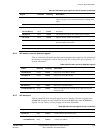
Read Data Channel
RDATAS[63:0] Output CLKIN Read data.
RIDS[7:0] Output CLKIN The identification tag for the read data group of signals.
RLASTS Output CLKIN Indicates the last transfer in a read burst.
RREADYS Input CLKIN Read ready signal indicating that the bus master can accept read
data and response information.
RRESPS[1:0] Output CLKIN Read response.
RVALIDS Output CLKIN Indicates address and control are valid.
Table A-6 AXI slave port signals for the L2 interface (continued)
Signal Direction Clocking Description
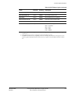
Table A-7 AXI slave port error detection signals
Signal Direction Clocking Description
AWPARITYS Input CLKIN Parity bit for write address channel
WPARITYS Input CLKIN Parity bit for write data channel
BPARITYS Output CLKIN Parity bit for write response channel
ARPARITYS Input CLKIN Parity bit for read address channel
RPARITYS Output CLKIN Parity bit for read data channel
AXISPARERR[2:0] Output CLKIN Parity error indication for read address (bit [2]), write data (bit [1]),
and write address (bit [0]) channels.


