


COPYRIGHT
©
1998 CANON INC. CANON NP7161/NP7160 REV.0 AUG. 1998 PRINTED IN JAPAN (IMPRIME AU JAPON)
4–7
CHAPTER 4 IMAGE FORMATION SYSTEM
E. Controlling the Developing/Separation Static Eliminator Bias
1. Outline
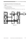
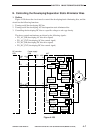
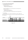
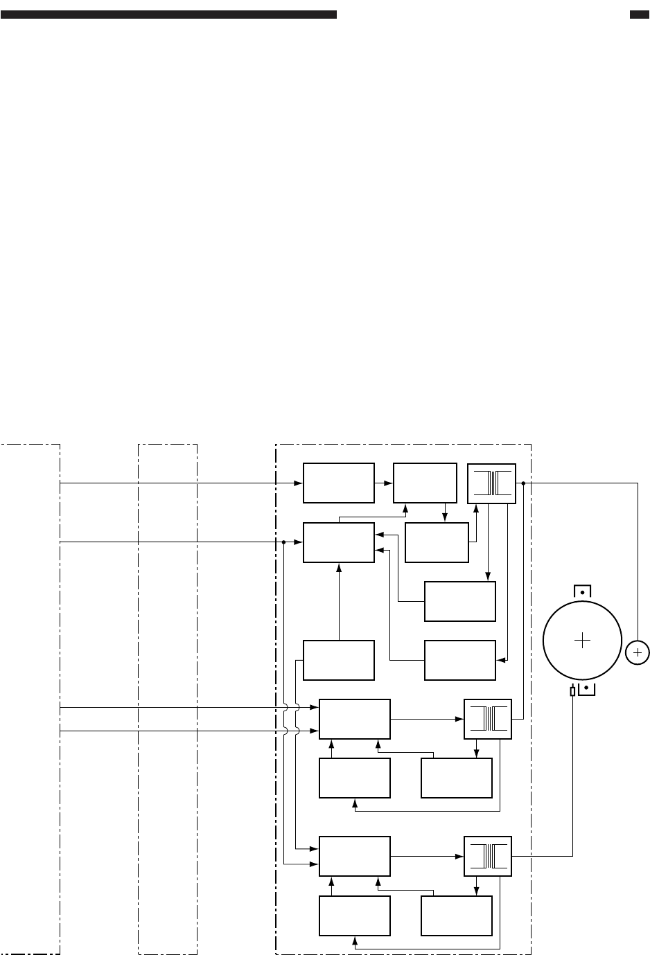
Figure 4-109 shows the circuit used to control the developing/static eliminating bias, and the
circuit has the following functions:
1. Turning on/off the developing DC bias
2. Turning on/off the developing AC bias/separation static eliminator bias
3. Controlling the developing DC bias to a specific voltage to suit copy density
The above control mechanisms are driven by the following signals:
•DV
_
AC
_
DR (developing AC bias drive signal)
•DV
_
AC
_
CNT (developing AC bias control signal)
•DV
_
DC
_
DR (developing DC bias drive signal)
•DV
_
DC
_
CNT (developing DC bias control signal)
Figure 4-109
Power supply
PCB
HVT
Sp
Dev
J301
-6
J210
-5
-7-4
-5-6
-4-7
Oscillation
control circuit
Short circuit
detection circuit
Voltage
detection circuit
Transformer
Oscillation
control circuit
Short circuit
detection circuit
Voltage
detection circuit
Transformer
Transformer
Frequency
switching circuit
Oscillation
circuit
Amplifier
circuit
Control
circuit
Reference
voltage circuit
Short circuit
detection circuit
Voltage
detection circuit
DC controller
PCB
J212
-12
J106
-13
DV
_
AC
_
CNT
-11-14
DV
_
AC
_
DR
-13-12
DV
_
DC
_
DR
-14-11
DV
_
DC
_
CNT