


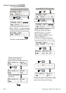
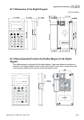
Appendix B Accessories|
B-24 Revision Nov. 2008, VLE1, SW V1.03
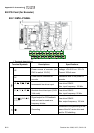
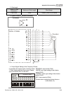
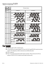
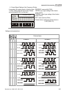
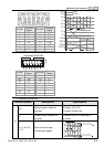
Settings and explanations
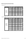
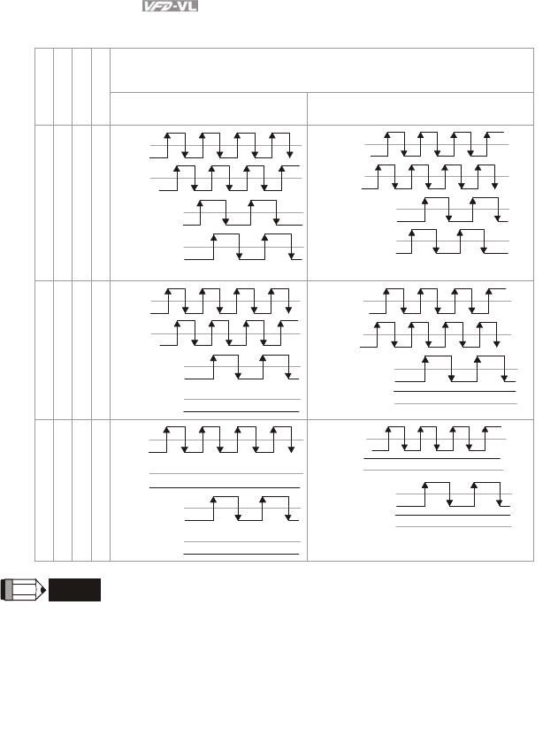
Division factor
RESERVE
I/MODE
O/MODE
RST
A leads B B leads A
X 0 0 1
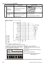
A-/A
B-/B
A/O-/A/O
B/O-/B/O
A-/A
B-/B
A/O-/A/O
B/O-/B/O
A/O-/A/O
B/O-/B/O
X 0 1 1
A-/A
B-/B
A/O-/A/O
B/O-/B/O
A/O-/A/O
B/O-/B/O
A-/A
B-/B
A/O-/A/O
B/O-/B/O
A/O-/A/O
B/O-/B/O
X 1 X 1
A-/A
B-/B
A/O-/A/O
B/O-/B/O
A/O-/A/O
B/O-/B/O
A-/A
B-/B
A/O-/A/O
B/O-/B/O
A/O-/A/O
B/O-/B/O
NOTE
When the switch is ON, it means logic 0.
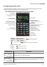
A-/A and B-/B are the input signals of PG card. A/O-/A/O and B/O-/B/O are the line driver
outputs of the frequency divider measured by the differential probe.
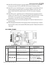
PIN1 is reserved.
PIN 5~12 are the denominator for the frequency divider. PIN 5 is the low bit (EX: the
setting of XXXX10101010 is that the input signal divides by 85).