


Appendix B Accessories|
Revision Nov. 2008, VLE1, SW V1.03 B-33
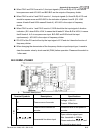
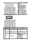
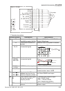
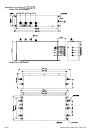
OB
A/O
A/O
B/O
B/O
OA
VP
0V
A+ (+COS)
B+ (+SIN)
Data+
EMVL-PGS01
CLOCK+
CLOCK-
A- (REFCOS)
B- (REFSIN)
PG
Data-
GND
Encoder
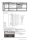
2. Terminals descriptions
Terminal Symbols Descriptions Specifications
VP Power source of encoder
(use SW2 to switch 12V/5V)
Voltage: +5VDC±5% or +8.3 VDC±6%
Current: 250mA max.
0V Power source common for
encoder
Reference level of the power of encoder
A+, A-,
B+, B-
Sine line drive input
(incremental signal)
Input frequency: 40kHz max.
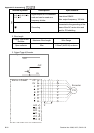
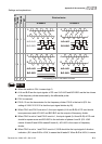
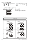
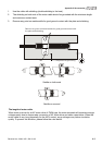
0
0
360 el.
0
90 el.
0
A
B
0.8....1.2Vss
(~
~
1Vss; Z =120 )
0
+SIN, +COS
REFSIN,
REFCOS
Sine line drive input
(incremental signal)
Input frequency: 20kHz max.
REFSIN/REFCOS
0.9...1.1V
SIN
CLOCK+,
CLOCK-
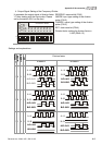
CLOCK line drive output Line Driver RS422 Level output
J3
Data+, Data- RS485 communication interface
Terminal resistor: about 130
Ω
TB1
A/O,
A
/O,
B/O,
B
/O
Signal output for PG
feedback card and can be
used as a frequency divider.
Line Driver RS422 Level output
OA
OB
Open collector output signal
and can be used as a
frequency divider
・Transistor open collector output
・Max. 24VDC, 30mA
・VOL≦1.5V(IOL=30mA)
・IOH≦200A(VOH=24VDC)
TB2
GND Open collector output
common
Reference level of NPN transistor open
collector output