


Appendix B Accessories|
Revision Nov. 2008, VLE1, SW V1.03 B-27
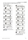
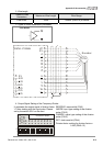
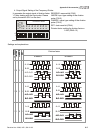
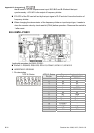
4. Output Signal Setting of the Frequency Divider
It generates the output signal of division factor
“n” after dealing with the input pulse. Please
set by the switch SW1 on the card.
ON
123
4
56789101112
RESERVE
I/MODE
O/MODE
RST
Division Factor
BIT0
BIT1
BIT2
BIT3
BIT4
BIT5
BIT6
BIT7
0
1
RESERVE: reserved bit (PIN1)
I/MODE: input type setting of the division
pulse (PIN 2)
O/MODE: output type setting of the division
pulse (PIN 3)
RST: clock reset bit (PIN 4)
Division factor: setting for division factor n:
1~256 (PIN5~12)
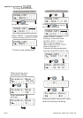
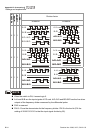
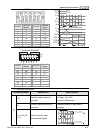
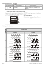
Settings and explanations
Division factor
RESERVE
I/MODE
O/MODE
RST
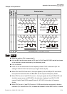
A leads B B leads A
X 0 0 1
A-/A
B-/B
A/O-/A/O
B/O-/B/O
A-/A
B-/B
A/O-/A/O
B/O-/B/O
A/O-/A/O
B/O-/B/O
X 0 1 1
A-/A
B-/B
A/O-/A/O
B/O-/B/O
A/O-/A/O
B/O-/B/O
A-/A
B-/B
A/O-/A/O
B/O-/B/O
A/O-/A/O
B/O-/B/O
X 1 X 1
A-/A
B-/B
A/O-/A/O
B/O-/B/O
A/O-/A/O
B/O-/B/O
A-/A
B-/B
A/O-/A/O
B/O-/B/O
A/O-/A/O
B/O-/B/O