


Appendix B Accessories|
B-28 Revision Nov. 2008, VLE1, SW V1.03
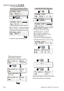
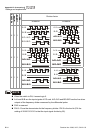
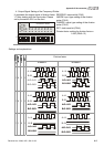
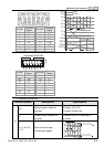
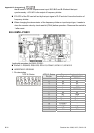
NOTE
When the switch is ON, it means logic 0.
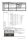
A-/A and B-/B are the input signals of PG card. A/O-/A/O and B/O-/B/O are the line driver
outputs of the frequency divider measured by the differential probe.
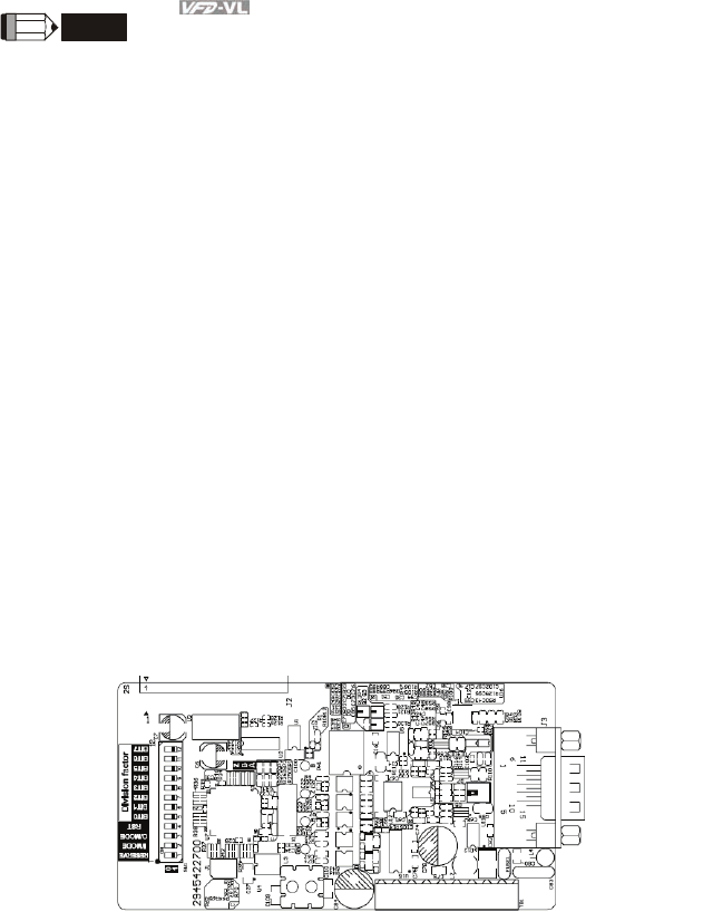
PIN1 is reserved.
PIN 5~12 are the denominator for the frequency divider. PIN 5 is the low bit (EX: the
setting of XXXX10101010 is that the input signal divides by 85).
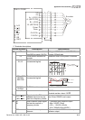
When PIN 2 and PIN 3 are set to 0, the input signals (A-/A and B-/B) of PG card should
be square wave and A/O-/A/O and B/O-/B/O are the outputs of frequency divider.
When PIN 2 is set to 0 and PIN 3 is set to 1, the input signals (A-/A and B-/B) of PG card
should be square wave and B/O-/B/O is the indication of phase A and B. (EX: LOW
means A leads B and HIGH means B leads A). A/O-/A/O is the output of frequency
divider.
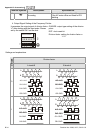
When PIN 2 is set to 1 and PIN 3 is set to X, B-/B should be the input signal of direction
indication. (EX: when B-/B is LOW, it means that A leads B. When B-/B is HIGH, it means
that B leads A. A-/A is a square wave input. B/O-/B/O and B-/B should be input
synchronously.
A/O-/A/O is the output of frequency divider.
Z/O-/Z/O of the PG card will act by the input signal of Z-/Z and don’t have the function of
frequency divider.
When changing the denominator of the frequency divider or input/output type, it needs to
clear the counter value by clock reset bit (PIN4) before operation. Please set the switch to
1 after reset.
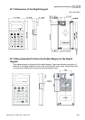
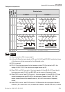
B.8.3 EMVL-PGH01 (only for Heidenhain ERN1387)
1. Sinusoidal Encoder Function