


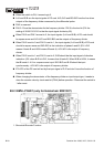

Appendix B Accessories|
B-32 Revision Nov. 2008, VLE1, SW V1.03
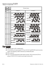
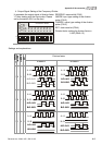
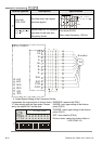
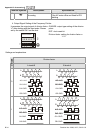
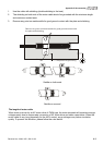
that B leads A. A-/A is a square wave input. B/O-/B/O and B-/B should be input
synchronously.
A/O-/A/O is the output of frequency divider.
Z/O-/Z/O of the PG card will act by the input signal of Z-/Z and don’t have the function of
frequency divider.
When changing the denominator of the frequency divider or input/output type, it needs to
clear the counter value by clock reset bit (PIN4) before operation. Please set the switch to
1 after reset.
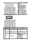
B.8.4 EMVL-PGS01
Applicable encoders for EMVL-PGS01:
EnDat2.1: EQN425, EQN1325, ECN113, ECN413, ECN1113, ECN1313
HIPERFACE: SRS50/60
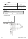
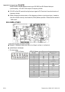
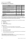
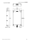
1. Pin description
Corresponding terminal
VFD-VL Series
Pin No.
EnDat HIPERFACE®
1 B- REFSIN
2 0V 0V
3 0V 0V
4 0V 0V
5 A+ +COS
6 A- REFCOS
7 0V 0V
8 B+ +SIN
9 VP VP
10 Data+ Data+
11 Data- Data-
12 CLOCK+ -
13 CLOCK- -
14 VP VP
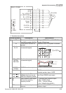
VFD-VL Series
5
4
3
2
1
10 9 8 7
6
15
14
13 12
11
15 0V 0V