


HYDRA
Service Manual
2A-20
The Totalizer Debounce circuit in the FPGA (A1U25) allows the Microprocessor to
select totalizing of either the input signal or the debounced input signal. The buffered
Totalizer Input signal (TOTI*) goes into the FPGA at A1U25-12. Inside the FPGA, the
totalizer signal is routed to the Totalizer Output (TOTO, A1U25-8) which then goes to a
16-bit counter in the Microprocessor (A1U1-114; TP20).
The actual debouncing of the input signal is accomplished by A1U25. Counters divide
the 12.288-MHz system clock down to 128 kHz for the debouncing circuit. An EXOR
gate compares the input signal (TOTI*) and the latched output of the debouncer. If these
signals differ, the EXOR gate output goes high, enabling the debouncer. If the input
remains stable for 1.75 milliseconds, the totalizer output (TOTO, A1U25-8) changes
state. If the input does not remain stable for 1.75 milliseconds, the totalizer output does
not change state. For a stable totalizer input of +5V dc, the totalizer output (TOTO,
A1U25-8) will be 0.0V dc. For a stable totalizer input of +0.0V dc, the totalizer output
(TOTO, A1U25-8) will be +5V dc.
2A-47. External Trigger Input Circuits
The External Trigger Input circuit can be configured by the Microprocessor to interrupt
on a rising or falling edge of the XT* input (A1J6-2) or to not interrupt on any
transitions of the XT* input. The falling edge of the XT* input is used by the instrument
firmware as an indication to start scanning, and the rising edge is used as an indication to
stop scanning.
The External Trigger Input is pulled up to +5V dc by A1Z2 and is protected from
electrostatic discharge (ESD) damage by A1R58, A1C54, A1Z3, and A1CR15. Capacitor
A1C54 helps ensure that the instrument meets EMI/EMC performance requirements.
The input (XTI) is then routed to the FPGA (A1U25), which contains the External
Trigger control circuitry. The Microprocessor sets control register bits in the FPGA
(A1U25) to control the external trigger circuit. The External Trigger control circuit
output (A1U25-9) drives the non-maskable interrupt on the Microprocessor (A1U1-95).
If External Triggering is enabled (see User Manual), the Microprocessor sets FPGA
control register bits to allow a low level on the XT* input to cause the External Trigger
Interrupt (XTINT*; A1U25-9) to go low. The Microprocessor then changes the FPGA
control register bits to allow a high level on the XT* input to cause XTINT* (A1U25-9)
to go low. Thus the Microprocessor can detect both rising and falling edges on the XT*
input. Normally, the XTINT* output of the FPGA (A1U25-9) should be low only for a
few microseconds at any time. If it is held low constantly, the instrument will not be able
to operate. Resistor A1R64 pulls the XTINT* output high to ensure that it is high during
power-up.
2A-48. A/D Converter PCA
The following paragraphs describe the operation of the circuits on the A/D Converter
PCA. The schematic for this pca is located in Section 8.
2A-49. Analog Measurement Processor
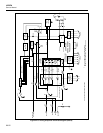
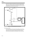
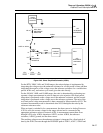
Refer to Figure 2A-3 for an overall picture of the Analog Measurement Processor chip
and its peripheral circuits. Table 2A-4 describes Analog Measurement Processor chip
signal names.
The Analog Measurement Processor (A3U8) is a 68-pin CMOS device that, under
control of the A/D Microcontroller (A3U9), performs the following functions:
• Input signal routing
• Input signal conditioning
• Range switching