


Theory of Operation (2635A)
Detailed Circuit Description
2A
2A-17
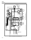
Clock Dividers
The 12.288-MHz system clock (A1U25-30) is divided down by the Clock Dividers to
create the 3.072-MHz Option Clock (OCLK; A1U25-22) and 1.024-MHz Display Clock
(DCLK; A1U25-19). The Display Clock is not a square wave; it is low for 2/3 of a cycle
and high for the other 1/3. The Display Clock is also used internal to the FPGA to create
the 128-kHz Totalizer Debouncer Clock and the 4-kHz Keyboard Scanner Clock.
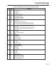
Internal Register Address Decoding
The FPGA logic decodes four bits of the address bus (A<3> through A<6>), the PGA*
chip select signal (A1U25-88), RDU* (A1U25-95), and WRU* (A1U25-5) to allow the
Microprocessor to read five registers and write to three registers implemented in the
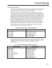
FPGA logic. The absolute addresses are listed in Table 2A-1.
Keyboard Scanner
The Keyboard Scanner sequences through the array of switches on the Display Assembly
to detect and debounce switch closures. After a switch closure is detected, it must remain
closed for at least 16 milliseconds before the Microprocessor will be interrupted and the
Keyboard Input register will be read from the FPGA. When the keyboard interrupt
(KINT*, A1U25-62) goes low, the Keyboard Scanner stops scanning until the
Microprocessor reads the Keyboard Input register which automatically clears the
interrupt by driving KINT* high again. The FPGA will interrupt the Microprocessor
again when the switch on the Display Assembly is detected as open again. Actually the
Microprocessor will be interrupted once for each debounced change in the contents of
the Keyboard Input register. See also the information on "Front Panel Switches" in the
"Display PCA" section for this instrument.
The Microprocessor can enable or disable the Keyboard Scanner by changing the state of
a bit in the Control/Status register that is in the FPGA. The Keyboard Scanner is disabled
if the instrument is in either the RWLS or LWLS state (see User Manual; RWLS and
LWLS Computer Interface Commands).
Digital I/O Buffers and Latches
The FPGA logic implements internal registers for the eight Digital Outputs (DO<0>
through DO<7>) and the four Alarm Outputs (AO<0> through AO<3>). These registers
are both written and read by the Microprocessor. The FPGA logic also implements an
eight-bit input buffer so that the Microprocessor can read the eight Digital Input lines
(DI<0> through DI<7>). See also "Digital Input Buffers" and "Digital and Alarm Output
Drivers".
Totalizer Debouncing and Mode Selection
Logic internal to the FPGA lets the Microprocessor enable a debouncer in the Totalizer
input signal path. The detailed description of the Totalizer Debouncer and Mode
Selection may be found under the heading "Totalizer Input".
External Trigger Logic
Logic internal to the FPGA allows the Microprocessor to set up the External Trigger
Logic to interrupt on rising or falling edges of the XTI input to the FPGA. The detailed