


Theory of Operation (2635A)
Detailed Circuit Description
2A
2A-11
The Display Reset signal (DRST*) is driven low by A1U2-6 when POR* is low, or it
may be driven low by the Microprocessor (A1U1-56) if the instrument firmware needs to
reset only the display hardware. For example, the firmware resets the display hardware
after the FPGA is loaded at power-up and the Display Clock (DCLK) signal from the
FPGA begins normal operation. This ensures that the Display Processor is properly reset
while DCLK is active.
The Option Reset signal (ORST*) is driven low by A1U2-3 when POR* is low, or it may
be driven low by the Microprocessor (A1U1-58) if the instrument firmware needs to
reset only the Option Interface hardware. For example, the firmware resets any option
interface hardware after the FPGA is loaded at power-up and the Option Clock (OCLK)
signal from the FPGA begins normal operation. This ensures that any Option Interface
hardware is properly reset while OCLK is active.
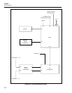
2A-33. Microprocessor
The Microprocessor uses a 16-bit data bus and a 19-bit address bus to access locations in
the Flash Memory (A1U14 and A1U16), the Nonvolatile Static RAM (A1U20 and
A1U24), the Real-Time Clock (A1U12), the FPGA (A1U25), the Memory Card
Interface PCA (A6), and the Option Interface (A1J1). All of the data bus lines and the
lowest 12 address lines have series termination resistors located near the Microprocessor
(A1U1) to ensure that the instrument meets EMI/EMC performance requirements. When
a memory access is done to the upper half of the data bus (D15 through D8), the upper
data strobe (UDS*) goes low. When a memory access is done to the lower half of the
data bus (D7 through D0), the lower data strobe (LDS*) goes low. When a memory
access is a read cycle, R/W* must be high. Conversely for any write cycle, R/W* must
be low.
The Microprocessor is a variant of the popular Motorola 68000 processor and is
enhanced by including hardware support for clock generation, address decoding, timers,
parallel ports, synchronous and asynchronous serial communications, interrupt
controller, DMA (Direct Memory Access) controllers, and a watchdog timer.
The 12.288-MHz system clock signal (A1TP11) is generated by the oscillator circuit
composed of A1U1, A1Y1, A1R2, A1C3, and A1C8. This clock goes through a series
termination resistor (A1R107) to the FPGA (A1U25) and also through another series
termination resistor (A1R86) to the Memory Card Interface (A1P4). These resistors are
necessary to ensure that the instrument meets EMI/EMC performance requirements.
The Microprocessor has four software programmed address decoders that include wait
state control logic. These four outputs are used to enable external memory and I/O
components during read and write bus cycles. See "Address Decoding" for a complete
description.
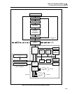
One sixteen-bit timer in the Microprocessor is used to generate a regular interrupt every
53.333 milliseconds. This timer uses the 12.288-MHz system clock (A1TP11) as a clock
source. The timer changes the state of parallel port pin A1U1-113 each time that it
interrupts the Microprocessor. The signal at A1U1-113 should be a 9.375-Hz square
wave (period of 106.67 milliseconds).
Another 16-bit timer is used as the totalizer counter. The totalizer signal originating at
J5-2 goes through the totalizer input buffer, the FPGA, and then to the external clock
input for this timer in the Microprocessor (U1-114 and TP20). See the Totalizer part of
"Digital I/O" for a complete description.
The Microprocessor has two parallel ports. Many of the parallel port pins are either used
as software controlled signals or as inputs or outputs of timers and serial communication
channels. Port A has 16 bits and Port B has 12 bits.