


Theory of Operation (2635A)
Detailed Circuit Description
2A
2A-15
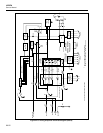
The SRAM* address decode output (A1U1-127) for the 128 kilobytes of NVRAM goes
low for any memory access to A1U20 or A1U24. This signal must go through two
NAND gates in A1U26 to the NVRAM chip select inputs (A1U20-22 and A1U24-22).
This ensures that when the instrument is powered down and A1U10-7 is driven low,
A1U20-22 and A1U24-22 will be driven high so that the contents of the NVRAM cannot
be changed and the power dissipated by the NVRAM is minimized. Jumper A1W4 in
A<18> is not used in the current instrument; it should be installed only if more NVRAM
is needed in a future instrument that needs 512 kilobytes of NVRAM using the same
circuit board. A1U24 is connected to the high 8 bits of the data bus, so read accesses are
enabled by the Read Upper (RDU*;A1U24-24) signal going low, and write accesses are
enabled by the Write Upper (WRU*;A1U24-29) signal going low. A1U20 is connected
to the low 8 bits of the data bus, so read accesses are enabled by the Read Lower
(RDL*;A1U20-24) signal going low, and write accesses are enabled by the Write Lower
(WRL*;A1U20-29) signal going low.
Memory accesses to the Real-Time Clock (A1U12) are enabled by the RTC* address
decode output (A1U11-16). This signal must go through two NAND gates in A1U26 to
the Real-Time Clock chip select input (A1U12-18). This ensures that when the
instrument is powered down and A1U10-7 is driven low, A1U12-18 will be driven high
so that the contents of the Real-Time Clock cannot be changed, and the power dissipated
by the Real-Time Clock is minimized. A1U12 is connected to the low 8 bits of the data
bus, so read accesses are enabled by the Read Lower (RDL*;A1U12-19) signal going
low, and write accesses are enabled by the Write Lower (WRL*;A1U12-20) signal going
low. When the instrument is powered up, the accuracy of the timebase generated by the
internal crystal may be tested by measuring the frequency of the 1-Hz square wave
output (A1U12-4). The Real-Time Clock also has an interrupt output (A1U12-3) that is
used by the Microprocessor to time the interval between scans when a scan interval is set
in the instrument. There should be one interrupt per second from the Real-Time Clock.
2A-37. Serial Communication (Guard Crossing)
The transmission of information from the Microprocessor (A1U1) to the Microcontroller
(A3U9) is accomplished via the circuit made up of A1Q10, A1U7, A1R8, A1R16, and
A3R8. The transmit output from the Microprocessor (A1U1-54) is buffered by A1Q10,
which then switches current through optocoupler LED (A1U7-2). Resistor A1R8 limits
the current through the LED.
The phototransistor in A1U7 responds to the light emitted by the LED when A1U1-54 is
driven low. (The collector of the phototransistor, A1U7-5, goes low.) The phototransistor
collector is pulled up by A3R8 on the A/D Converter PCA. When turning off, the
phototransistor base discharges through A1R16. With this arrangement, the rise and fall
times of the phototransistor collector signal are nearly symmetrical.
The transmission of data from the Microcontroller (A3U9) to the Microprocessor
(A1U1) is accomplished via the circuit made up of A3Q1, A3R7, A1U5, A1R7, and
A1R3. The transmit output from the Microcontroller (A3U9-14) is inverted by A3Q1,
which drives the optocoupler LED (A1U5-2) through resistor A3R7. The current through
the LED is limited by resistor A3R7. The phototransistor in A1U5 responds to the light
emitted by the LED when A1U5-2 is driven low. (The collector of the phototransistor,
A1U5-4, goes low.) The phototransistor collector (A1U5-5) is pulled up by resistor
A1R3. When turning off, the phototransistor base discharges through A1R7. With this
arrangement, the rise and fall times of the phototransistor collector signal are nearly
symmetrical.