


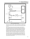

Theory of Operation (2620A/2625A)
Detailed Circuit Description
2
2-19
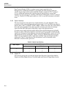
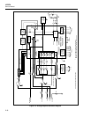
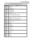
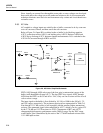
Table 2-4. Analog Measurement Processor Pin Descriptions
Pin Name Description
1
2
3
4
5
VDD
ACBO
AIN
AGND2
ACR4
+5.4V supply
AC buffer output
(not used)
Analog ground
AC buffer range 4 (300V)
6
7
8
9
10
ACR3
ACR2
ACR1
VSSA
REFJ
AC buffer range 3 (30V)
AC buffer range 2 (3V)
AC buffer range 1 (300 mV)
-5.4V supply for AC ranging
Reference junction input
11
12
13
14
15
DCV
LOW
GRD
RRS
V4
V3
A/D converter low input
Driven guard
Reference resistor sense for ohms
Tap #4 on the DCV input divider/ohms reference network
Tap #3 on the DCV input divider/ohms reference network
16
17
18
19
20
V1
GRD
V2F
V2
GRD
Tap #1 on the DCV input divider/ohms reference network
Driven guard
Tap #2 input on the DCV input divider/ohms reference network
Tap #2 on the DCV input divider/ohms reference network
Driven guard
21
22
23
24
25
V0
GRD
OVS
GRD
AGND1
Tap #0 on the DCV input divider/ohms reference network
Driven guard
Ohms and volts sense input
Guard
Analog ground
26
27
28
29
30
-
DGND
FC0
FC1
FC2
(not used)
Analog ground
Function control #0
Function control #1
Function control #2
31
32
33
34
35
FC3
FC4
FC5
FC6
FC7
Function control #3
(not used)
(not used)
Function control #6
Function control #7
36
37
38
39
40
XIN
XOUT
MRST
AS
AR
Crystal oscillator input
Crystal oscillator output
Master reset
Analog send
Analog receive
41
42
43
44
45
SK
CS
BRS
VSS
INT
Serial clock
Chip select
(not used)
-5.4V dc
Integrator output