


Diagnostic Testing and Troubleshooting (2620A/2625A)
Display Assembly Troubleshooting
5
5-23
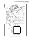
5-18. Display Assembly Troubleshooting
The following discussion is helpful if it has been determined that the Display Assembly
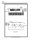
is faulty. Refer to Figure 5-8 for Display PCA test points. This initial determination may
not be arrived at easily, since an improperly operating display may be the result of a
hardware or software problem that is not a direct functional part of the Display
Assembly. Consult the General Troubleshooting Procedures found earlier in this section
for procedures to isolate the fault to the Display Assembly. Use the following discussion
of display software operation when troubleshooting problems within a known faulty
Display Assembly. A Display Extender Cable (PN 867952) is available for use during
troubleshooting. Note that this cable must be twisted to mate correctly to the connectors
on Display and Main PCAs.
The Display Controller reads the DTEST* and LTE* inputs to determine how to
initialize the display memory. DTEST* and LTE* default to logic 1 and logic 0,
respectively, to cause all display segments to be initialized to "on". DTEST* is
connected to test points A2TP4, and LTE* is connected to A2TP5. Either test point can
be jumpered to VCC (A2TP6) or GND (A2TP3) to select other display initialization
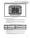
patterns. Display Test Patterns #1 and #2 are a mixture of "on" and "off" segments with a
recognizable pattern to aid in troubleshooting problems involving individual display
segments. When either of the special display patterns is selected, the beeper is also
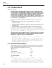
sounded for testing without interaction with the Microprocessor. Table 5-8 indicates the
display initialization possibilities.
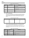
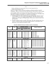
Table 5-8. Display Initialization
A2TP4 DTEST* A2TP5 LTE* POWER-UP DISPLAY INITIALIZATION
1
1
0
0
1
0
1
0
All Segments OFF
All Segments ON (default)
Display Test Pattern #1
Display Test Pattern #2
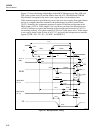
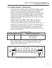
Figure 5-9 shows the timing of communications between the Microprocessor and the
Display Controller. Figures 5-10 and 5-11 show Display Test Patterns #1 and #2,
respectively. Refer to the Display Assembly schematic diagram in Section 8 for
information on grid and anode assignments.
BIT 7
BIT 7
HOLD OFF
CLEAR TO
RECEIVE
26 µs
DISTX
DSCLK
DISRX
CLEAR TO
RECEIVE
26 µs
BIT 6 BIT 5 BIT 4 BIT 3 BIT 2 BIT 1 BIT 0
BIT 6 BIT 5 BIT 4 BIT 3 BIT 2 BIT 1 BIT 0
s40f.eps
Figure 5-9. Display Controller to Microprocessor Signals