


Theory of Operation (2620A/2625A)
Detailed Circuit Description
2
2-15
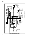
2-44. Digital Input Threshold 2-1.
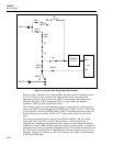
The Digital Input Threshold circuit sets the input threshold level for the Digital Input
Buffers and the Totalizer Input. A software programmable voltage divider (A1U17,
A1R35, A1R36, A1R37) and a unity gain buffer amplifier (A1AR1) are the main
components in this circuit. The Microprocessor sets outputs A1U16-15 and A1U16-12 to
select one of four input threshold levels. These outputs control the resistive divider
(A1R35, A1R36, A1R37) via two drivers with open-collector outputs in A1U17. The
voltage from the divider is then buffered by A1AR1 which sets the input threshold.
Capacitor A1C29 filters the divider voltage at the input of A1AR1. Table 2-3 defines the
programmable input threshold levels.
The instrument selects the +1.4V dc threshold level at power-up initialization.
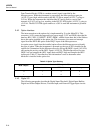
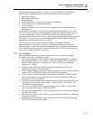
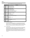
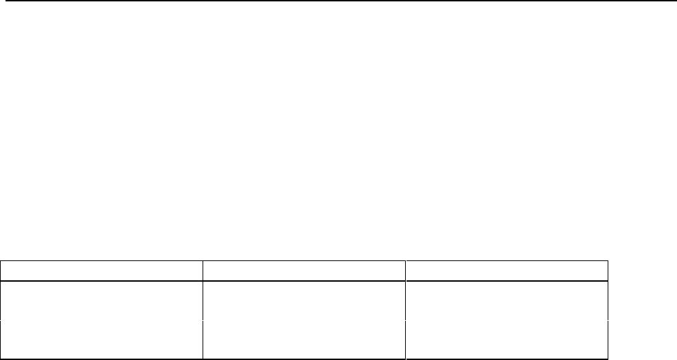
Table 2-3. Programmable Input Threshold Levels
A1U16-15 A1U16-12 Input Threshold Voltage
00+2.5V dc
01+0.7V dc
10+1.4V dc
11+0.7V dc
2-45. Digital Input Buffers
Since the eight Digital Input Buffers are identical in design, only components used for
Digital Input 0 are referenced in this description. If the Digital Output Driver (A1U27-
16) is off, the input to the Digital Input Buffer is determined by the voltage level at
A1J5-10. If the Digital Output Driver is on, the input of the Digital Input Buffer is the
voltage at the output of the Digital Output Driver.
The Digital Input Threshold circuit and resistor network A1Z1 determine the input
threshold voltage and hysteresis for inverting comparator A1AR2. The inverting input of
the comparator (A1AR2-2) is protected by a series resistor (A1Z3) and diode A1CR14.
A negative input clamp circuit (A1Q9, A1Z2, and A1CR17) sets a clamp voltage of
approximately +0.7V dc for the protection diodes of all Digital Input Buffers. A negative
input voltage at A1J5-10 causes A1CR14 to conduct current, clamping the comparator
input A1AR2-2 at approximately 0V dc.
The input threshold of +1.4V dc and a hysteresis of +0.5V dc are used for all Digital
Input Buffers. When the input of the Digital Input Buffer is greater than approximately
+1.65V dc, the output of the inverting comparator is low. When the input then drops
below about +1.15V dc, the output of the inverting comparator goes high.
2-46. Digital and Alarm Output Drivers
Since the 12 Digital Output and Alarm Output Drivers are identical in design, the
following example description references only the components that are used for Alarm
Output Driver 0.
The Microprocessor controls the state of Alarm Output Driver 0 by writing to latch
output A1U16-2. When A1U16-2 is set high, the output of the open-collector Darlington
driver (A1U17-15) sinks current through current limiting resistor A1R62. When A1U16-
2 is set low, the driver output turns off and is pulled up by A1Z2 and/or the voltage of
the external device that the output is driving. If the driver output is driving an external
inductive load, the internal flyback diode (A1U17-9) conducts the energy into MOV
A1RV1 to keep the driver output from being damaged by excessive voltage. Capacitor
A1C58 ensures that the instrument meets electromagnetic interference (EMI) and
electromagnetic compatibility (EMC) performance requirements.