


HYDRA
Service Manual
2-10
amplifier. A1VR2 is the reference for the positive supply. A1R14 provides the current to
bias the reference zener. A1C4 is the output filter, and A1C9 provides frequency
compensation of the regulator circuit. Transistor A1Q1 and resistor A1R13 make up the
current-limit circuit.
When the voltage across A1R13 increases enough to turn on A1Q1, output current is
limited by removing the base drive to A1Q2.
The -5.4 volt regulator operates like the +5.3 volt regulator, except that the NPN
transistors in the positive supply are PNP transistors in the negative supply, and the PNP
transistors in the positive supply are NPN transistors in the negative supply. If a VDD-
to-VSS short circuit occurs, diode A1CR4 ensures that current limit occurs at the limit
set for the -5.4V dc or +5.3V dc supply, whichever is lower.
2-31. Power Fail Detection
The power fail detection circuit generates a signal to warn the Microprocessor that the
power supply is going down. Comparator A1U24 compares the divided-down raw
supply voltage and the band-gap generated reference voltage. When the raw supply
voltage is greater than about 8V dc, the output of A1U24 is "high" and when the raw
supply falls below 8V dc, the output goes "low". Resistors A1R39 and A1R41 make up
the divider, and resistor A1R43 provides bias for the band-gap reference. Resistor
A1R42 is a pull up resistor for the comparator output, and resistor A1R45 provides
positive feedback to provide the comparator with some hysteresis.
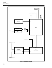
2-32. Digital Kernel
The Digital Kernel is composed of the following eight functional circuit blocks: the
Microprocessor, the ROM (Read-Only Memory), the NVRAM/Clock (Nonvolatile
Random Access Memory and Real-Time Clock), the EEPROM (Electrically Erasable
Programmable Read-Only Memory), the Counter/Timer, the RS-232 Interface, and the
Option Interface.
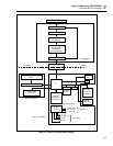
2-33. Microprocessor
The Microprocessor uses an eight-bit data bus and a sixteen-bit address bus to access
memory locations in the ROM (A1U8), the NVRAM/Clock (A1U3), the Counter/Timer
(A1U2), the Digital I/O Registers (A1U13, A1U16, A1U26), the Memory PCA (A6),
and the IEEE-488 PCA (A5).
The Microprocessor oscillator operates at a 4.9152-MHz frequency determined by
crystal A1Y1. The A1U4-68 system clock signal (the Microprocessor oscillator
frequency divided by four) is a square wave with a frequency of 1.2288 MHz. This
system clock also determines the memory cycle time of 0.813 microseconds. The system
clock is also used by the Display Assembly and the IEEE-488 option assembly after
being damped by series resistor A1R19 to minimize the EMI generated by this signal’s
sharp edges.
When the address bus is stable, the Microprocessor enables either the reading of memory
(by driving RD*, A1U4-67, low) or writing of memory (by driving WR*, A1U4-66,
low.)
The Microprocessor uses a three-wire synchronous communication interface to store and
retrieve instrument communication configuration and calibration information in the
EEPROM (A1U1). See the EEPROM description for more detailed information.
The Microprocessor communicates to the Display Controller using another synchronous,
three-wire communication interface described in detail in the Display Controller Theory
of Operation in this section.