Theory of Operation (2620A/2625A)
Detailed Circuit Description
2
2-33
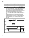
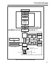
1.14 ms
0V
5V
ANODE(14..0)
-30V
GRID(X)
-30V
GRID(X-1)
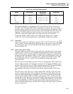
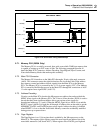
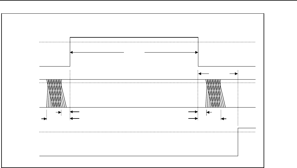
GRID/ANODE TIMING
5V
-30V
60 µs
19 µs
98 µs
56 µs
116 µs
0V
5V
0V
s10f.eps
Figure 2-10. Grid-Anode Timing Relationships
2-71. Memory PCA (2625A Only)
The Memory PCA is a serially-accessed, byte-wide, nonvolatile 256K-byte memory that
is capable of storing up to 2047 scans of data. The following paragraphs describe in
detail the Main PCA Connector, Address Decoding, Page Register, Byte Counter, and
Nonvolatile Memory blocks that make up this assembly.
2-72. Main PCA Connector
The Memory PCA interfaces to the Main PCA through a 26-pin, right angle connector
(A6J1). This connector routes the eight-bit data bus, the lower three bits of the address
bus, memory control and address decode signals from the Main PCA to the Memory
PCA. The Memory PCA is powered by the +5.1V dc power supply (VCC). The Memory
PCA is sensed by the Microprocessor on the Main PCA through the connection of A6J1-
11 to the option sense signal OPS* (A6J1-22).
2-73. Address Decoding
Circuitry on the Main PCA decodes the Microprocessor address bus and provided the
MEM* select signal to the Memory PCA. The 3-line to 8-line decoder (A6U8) is used to
decode the three least significant address bits to get register select signals for
hexadecimal addresses 4, 5, and 6. When the MEM* signal drives A6U8-4 low and the
RESET* signal (A6U8-6) is high, the A0 through A2 address bits are decoded to get the
MEMORY, PAGEL, and PAGEH register select signals.Address decoding is disabled
when RESET* is low so that the Nonvolatile Memory cannot be accidentally modified
during power-up or power-down.
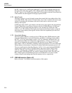
2-74. Page Register
The Page Register is an 11-bit register that is writable by the Microprocessor on the
Main PCA. The outputs of this register control the most significant address bits of the
nonvolatile memories (A6U6 and A6U7.) When register select PAGEL goes high and


