


Theory of Operation (2635A)
Detailed Circuit Description
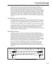
2A
2A-29
A3K15
INPUT LO
A3R43
A3U7
+
_
A3Z3
1.111M
A3Z3
115.7
A3Z3 FEEDBACK
RESISTOR
A3Z3
2.776k
RMS
COVERTER
A3C15
&
A3C16
A3R11
A3U6
INPUT HI
A3R44
A3C31
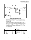
s16f.eps
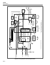
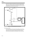
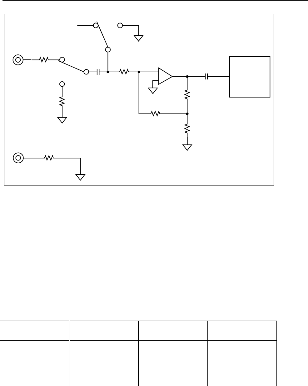
Figure 2A-6. AC Buffer Simplified Schematic (2635A)
JFETs A3Q3 through A3Q9 select one of the four gain (or attenuation) ranges of the
buffer (wide-bandwidth op-amp A3U7.) The four JFET drive signals ACR1 through
ACR4 turn the JFETs on at 0V and off at -VAC. Only one line at a time will be set at 0
volts to select a range.
The input signal to the buffer is first divided by 10, 100, or 1000 for the 300 mV, 3V,
and 30V ranges, respectively. The resistance ratios used are summarized in Table 2A-6.
Note that the 111.1-kΩ resistor is left in parallel with the smaller (higher attenuation)
resistors. The attenuated signal is then amplified by A3U7, which is set for a gain of 25
by the 2.776-kΩ and 115.7Ω resistors in A3Z3. Components A3R27 and A3C23
compensate high-frequency performance on the 300 mV range. For the 300V range,
overall buffer gain is determined by the ratio of the 2.776-kΩ feedback resistor to the
1.111-MΩ input resistor.
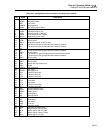
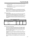
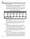
Table 2A-6. AC Volts Input Signal Dividers (2635A)
Range Drive Signal A3Z3 Divider
Resistor(s)
Overall Gain
300 mV ACR1 111.1 kΩ 2.5
3V ACR2 12.25 kΩ || 111.1 kΩ 0.25
30V ACR3 1.013 kΩ || 111.1 kΩ 0.025
150/300V ACR4 none 0.0025