


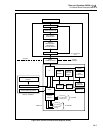

Theory of Operation (2635A)
Detailed Circuit Description
2A
2A-9
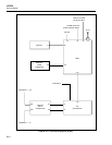
The output voltage of the switcher supply is controlled by varying the duty cycle (ON
time) of the switching transistor in the controller/switch device A1U9. A1U9 contains
the supply reference, oscillator, switch transistor, pulse-width modulator comparator,
switch drive circuit, current-limit comparator, current-limit reference, and thermal limit.
Dual inductor A1T2 regulates the current that flows from the raw supply to the load as
the switching transistor in A1U9 is turned on and off. Complementary switchA1CR10
conducts when the switching transistor is off.
The pulse-width modulator comparator in A1U9 compares the output to the reference
and sets the ON-time/OFF-time ratio to regulate the output to 5.1V dc. A1C26 is the
input filter capacitor, and A1C14 is the output filter capacitor. Proper inductor and
capacitor values set the filter frequency response to ensure best overall system stability.
Circuitry consisting of A1R26, A1C21, and A1C18 ensure that the switcher supply
remains stable and operating in the continuous mode. Resistors A1R30 and A1R31 set
the output voltage to within 5% of 5.1V.Capacitor A1C21 sets the operating frequency
of the switcher at approximately 100 kHz.
Resistors A1R30 and A1R31 form a voltage divider that operates in conjunction with
amplifier A1U28, which is configured as a voltage follower.A1U28-5 samples the 5.1V
dc output, while A1U28-6 is the voltage divider input.The effect is to maintain the
junction of R30 and R31 at 5.1V dc, resulting in an A1U28-7 output level of 6.34V dc,
or 1.24V dc above the output.This feedback voltage is applied to A1U9-2, which A1U9
interprets as 1.24V dc because A1U9-3 (ground) is connected to the 5.1V dc output.
A1U9 maintains the feedback and reference voltages at 1.24V dc and thus regulates the
5.1V dc source.
2A-27. Inverter
The inverter supply uses a two transistor driven push-pull configuration. The center tap
of transformer A1T1 primary is connected to the 5.0V dc VCC supply, and each side is
alternately connected to common through transistors A1Q7 and A1Q8. A1R38 may be
removed to disable the inverter supply for troubleshooting purposes. A1Q7 and A1Q8
are driven by the outputs of D flip-flop A1U22. Resistors A1R34 and A1R28, and diodes
A1CR11 and A1CR12 shape the input drive signals to properly drive the gate of the
transistors. D flip-flop A1U22 is wired as a divide-by-two counter driven by a 110-kHz
square wave. The 110-kHz square wave is generated by hex inverter A1U23, which is
connected as an oscillator with a frequency determined by the values of resistors A1R40
and A1R47 and capacitor A1C35. The resulting ac voltage produced across the
secondary of A1T1 is rectified to provide the input to the inverter inguard and outguard
supplies.
2A-28. Inverter Outguard Supply
The inverter outguard supply provides three outputs: 5.4V ac, -30V dc, and -5V dc.
These voltages are required by the display and RS-232 drivers and receiver. The 5.4V ac
supply comes off the secondary windings (pins 6 and 7) on transformer T1, and it is
biased at -24V dc with zener diode A1VR3 and resistor A1R22. Dual diodes A1CR8 and
A1CR9 and capacitor A1C17 are for the -30V dc supply. Capacitors A1C30 and A1C31,
and dual diodes A1CR13 form a voltage doubler circuit that generates -12 volts. Three-
terminal regulator A1U18 then regulates this voltage down to -5V for the RS-232 circuit.
Capacitor A1C32 is needed for transient response performance of the three-terminal
regulator.