


Theory of Operation (2635A)
Detailed Circuit Description
2A
2A-13
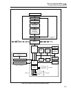
2A-34. Address Decoding
The four chip-select outputs on the Microprocessor are individual software programmed
elements that allow the Microprocessor to select the base address, the size, and the
number of wait states for the memory accessed by each output.
The FLASH* signal (A1U1-128) enables accesses to 128 kilobytes of Flash Memory
(A1U14 and A1U16). The FLASH* signal goes through jumper W3, which must always
be installed during normal instrument operation. W3 is removed only during the initial
programming of the Flash Memory during production at the factory. The SRAM* signal
enables the Nonvolatile Static RAM (A1U20 and A1U24), and the MCARD* signal goes
to the Memory Card Interface PCA (A6). The I/O* signal goes to the I/O Decoder
(A1U11), which decodes small areas of address space for I/O devices like the FPGA, the
Real-Time Clock, and the Option Interface. There are no wait states for accesses to
FLASH* and SRAM*, but two wait states are used for any access to I/O*. Each wait
state adds approximately 83 nanoseconds to the length of a memory read or write cycle.
The Memory Card Interface handles wait state timing for any accesses to MCARD*.
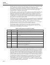
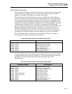
When the Microprocessor is starting up (also referred to as "booting"), the address
decoding maps the address space as shown in Table 2A-2.
Table 2A-2. Booting Microprocessor Memory Map (2635A)
Hexadecimal Address Device Selected
000000 - 03FFFF
100000 - 13FFFF
300000 - 30007F
300080 - 3000FF
300100 - 30017F
310000 - 311FFF
400000 - 401000
Flash (A1U14 and A1U16)
NVRAM (A1U20 and A1U24)
FPGA Configuration (A1U25)
Real-Time Clock (A1U12)
Option Interface (A1J1)
Memory Card Interface (A1P4)
Microprocessor Internal
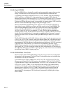
Just before beginning execution of the instrument code, the address decoding is changed
to map the address space as shown in Table 2A-3. This change switches the positions of
Flash Memory and Nonvolatile Static RAM within the address space of the
Microprocessor.
Table 2A-3. Instrument Microprocessor Memory Map (2635A)
Hexadecimal Address Device Selected
000000 - 03FFFF
100000 - 13FFFF
300000 - 300007
300008 - 30000F
300010 - 300017
300018 - 30001F (Read Only)
300020 - 300027 (Read Only)
300080 - 3000FF
300100 - 30017F
310000 - 311FFF
400000 - 401000
NVRAM (A1U20 and A1U24)
Flash (A1U14 and A1U16)
FPGA Control / Status (A1U25)
Alarm Outputs (A1U25)
Digital Outputs (A1U25)
Digital Inputs (A1U25)
Keyboard Input (A1U25)
Real-Time Clock (A1U12)
Option Interface (A1J1)
Memory Card Interface (A1P4)
Microprocessor Internal