


HYDRA
Service Manual
2A-16
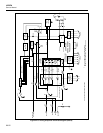
2A-38. Display/Keyboard Interface
The Microprocessor sends information to the Display Processor via a three-wire
synchronous communication interface. The detailed description of the DISTX, DISRX,
and DSCLK signals may be found in the detailed description of the Display PCA. Note
that the DISRX signal is pulled down by resistor A1R1 so that Microprocessor inputs
A1U1-49 and A1U1-118 are not floating at any time.
The Display Clock (DCLK) is a 1.024-MHz clock that is generated by the FPGA. Series
resistor A1R85 is necessary to ensure that the instrument meets EMI/EMC performance
requirements. The Display Assembly is reset when the Display Reset (DRST*) signal is
driven low. The reset circuit on the Display Assembly is discharged through resistor
A1R21, which limits the peak current from A2C3. DRST* is driven low at power-up, or
it may be driven low by the Microprocessor (A1U1-56).
The Keyboard interface is made up of six bidirectional I/O lines from the Field
Programmable Gate Array (FPGA). SWR1 through SWR6 (A1U25-67, A1U25-68,
A1U25-71, A1U25-73, A1U25-70, A1U25-69, respectively) are pulled up by A2Z1 on
the Display PCA. Hardware in the FPGA scans the keyboard switch array, detects and
debounces switch changes, and interrupts the Microprocessor to indicate that a
debounced keypress is available. A detailed description of this may be found under the
following heading "Field Programmable Gate Array (FPGA)".
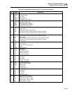
2A-39. Field Programmable Gate Array (FPGA)
The FPGA is a complex programmable logic device that contains the following six
functional elements after the Microprocessor has loaded the configuration into the
FPGA: Clock Dividers, Internal Register Address Decoding, Keyboard Scanner, Digital
I/O Buffers and Latches, Totalizer Debouncing and Mode Selection, and the External
Trigger Logic.
When the instrument is powered up, the FPGA clears its configuration memory and
waits until RESET* (A1U25-78) goes high. The FPGA then tests its mode pins and
should determine that it is in "peripheral" configuration mode (A1U25-54 high; A1U25-
52 low; A1U25-56 high). In this mode the Microprocessor must load the configuration
information into the FPGA before the FGPA logic can begin operation.
The Microprocessor first makes sure that the FPGA is ready to be configured by driving
XD/P* (A1U25-80) low and then pulsing the RESET* (A1U25-78) input low for about
10 microseconds. The Microprocessor then waits until the XINIT* (A1U25-65) output
goes high, indicating that the FPGA has been initialized and is ready for configuration.
The Microprocessor then writes a byte of configuration data to the FPGA by driving
PGA* (A1U25-88) low and latching the data on the data inputs (D<8> through D<15>)
by pulsing WRU* (A1U25-5) low and then back high. The XRDY (A1U25-99) output
then goes low to indicate that the FPGA is busy loading that configuration byte. The
Microprocessor will then wait until XRDY goes high again before loading the next
configuration byte, and the sequence is repeated until the last byte is loaded. While the
configuration data is being loaded, the FPGA drives the XD/P* signal (A1U25-80) low.
When the FPGA has been completely configured, the XD/P* signal is released and
pulled high by resistor A1R70. The Microprocessor will repeat the configuration
sequence if XD/P* (A1U25-80) does not go high when it is expected to.